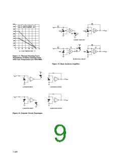
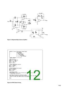
Balance control R1 adjusts the
relative gain for the positive and
negative portions of the input
signal, gain control R7 adjusts the
overall gain of the isolation
amplifier, and capacitors C1-C3
provide compensation to stabilize
the amplifiers.
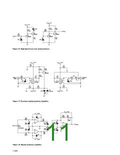
decrease at low input voltages
and LED currents. This would
reduce the loop gain of the input
circuit, reducing circuit accuracy
and bandwidth. D1 prevents
excessive reverse voltage from
being applied to the LED when
the LED turns off completely.
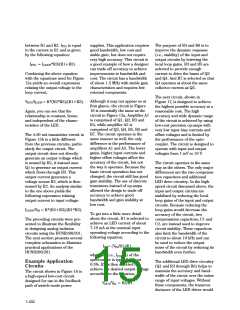
terminal of input photodiode PD1
to allow bipolar input currents.
Normally the forward voltage
drops of the diodes would cause a
serious linearity or accuracy
problem. However, an additional
amplifier is used to provide an
appropriate offset voltage to the
other amplifiers that exactly
cancels the diode voltage drops to
maintain circuit accuracy.
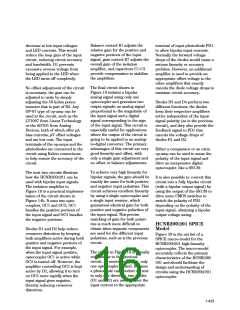
The final circuit shown in
Figure 19 isolates a bipolar
analog signal using only one
No offset adjustment of the circuit
is necessary; the gain can be
adjusted to unity by simply
adjusting the 50 kohm poten-
tiometer that is part of R2. Any
OP-97 type of op-amp can be
used in the circuit, such as the
LT1097 from Linear Technology
or the AD705 from Analog
Devices, both of which offer pA
bias currents, µV offset voltages
and are low cost. The input
terminals of the op-amps and the
photodiodes are connected in the
circuit using Kelvin connections
to help ensure the accuracy of the
circuit.
optocoupler and generates two
output signals: an analog signal
proportional to the magnitude of
the input signal and a digital
signal corresponding to the sign
of the input signal. This circuit is
especially useful for applications
where the output of the circuit is
going to be applied to an analog-
to-digital converter. The primary
advantages of this circuit are very
good linearity and offset, with
only a single gain adjustment and
no offset or balance adjustments.
Diodes D3 and D4 perform two
different functions; the diodes
keep their respective amplifiers
active independent of the input
signal polarity (as in the previous
circuit), and they also provide the
feedback signal to PD1 that
cancels the voltage drops of
diodes D1 and D2.
Either a comparator or an extra
op-amp can be used to sense the
polarity of the input signal and
drive an inexpensive digital
optocoupler, like a 6N139.
To achieve very high linearity for
bipolar signals, the gain should be
exactly the same for both positive
and negative input polarities. This
circuit achieves excellent linearity
by using a single optocoupler and
a single input resistor, which
guarantees identical gain for both
positive and negative polarities of
the input signal. This precise
matching of gain for both polari-
ties is much more difficult to
obtain when separate components
are used for the different input
polarities, such as is the previous
circuit.
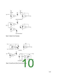
The next two circuits illustrate
how the HCNR200/201 can be
used with bipolar input signals.
The isolation amplifier in
Figure 18 is a practical implemen-
tation of the circuit shown in
Figure 14b. It uses two opto-
couplers, OC1 and OC2; OC1
handles the positive portions of
the input signal and OC2 handles
the negative portions.
It is also possible to convert this
circuit into a fully bipolar circuit
(with a bipolar output signal) by
using the output of the 6N139 to
drive some CMOS switches to
switch the polarity of PD2
depending on the polarity of the
input signal, obtaining a bipolar
output voltage swing.
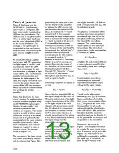
HCNR200/201 SPICE
Model
Diodes D1 and D2 help reduce
crossover distortion by keeping
both amplifiers active during both
positive and negative portions of
the input signal. For example,
when the input signal positive,
optocoupler OC1 is active while
OC2 is turned off. However, the
amplifier controlling OC2 is kept
active by D2, allowing it to turn
on OC2 more rapidly when the
input signal goes negative,
Figure 20 is the net list of a
SPICE macro-model for the
HCNR200/201 high-linearity
optocoupler. The macro-model
accurately reflects the primary
characteristics of the HCNR200/
201 and should facilitate the
design and understanding of
circuits using the HCNR200/201
optocoupler.
The circuit in Figure 19 is actually
very similar to the previous
circuit. As mentioned above, only
one optocoupler is used. Because
a photodiode can conduct current
in only one direction, two diodes
(D1 and D2) are used to steer the
input current to the appropriate
thereby reducing crossover
distortion.
1-433

 AGILENT [ AGILENT TECHNOLOGIES, LTD. ]