between R1 and R3. IPD1 is equal
to the current in R1 and is given
by the following equation:
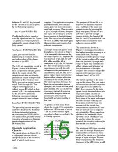
supplies. This application requires
good bandwidth, low cost and
stable gain, but does not require
very high accuracy. This circuit is
a good example of how a designer
can trade off accuracy to achieve
improvements in bandwidth and
cost. The circuit has a bandwidth
of about 1.5 MHz with stable gain
characteristics and requires few
external components.
The purpose of R4 and R6 is to
improve the dynamic response
(i.e., stability) of the input and
output circuits by lowering the
local loop gains. R3 and R5 are
selected to provide enough
current to drive the bases of Q2
and Q4. And R7 is selected so that
Q4 operates at about the same
collector current as Q2.
IPD1 = ILOOP*R3/(R1+R3).
Combining the above equation
with the equations used for Figure
12a yields an overall expression
relating the output voltage to the
loop current,
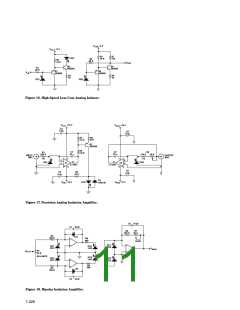
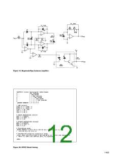
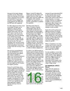
The next circuit, shown in
Although it may not appear so at
first glance, the circuit in Figure
16 is essentially the same as the
circuit in Figure 12a. Amplifier A1
is comprised of Q1, Q2, R3 and
R4, while amplifier A2 is
VOUT/ILOOP = K*(R2*R3)/(R1+R3).
Figure 17, is designed to achieve
the highest possible accuracy at a
reasonable cost. The high
Again, you can see that the
relationship is constant, linear,
and independent of the charac-
teristics of the LED.
accuracy and wide dynamic range
of the circuit is achieved by using
low-cost precision op-amps with
very low input bias currents and
offset voltages and is limited by
the performance of the opto-
coupler. The circuit is designed to
operate with input and output
voltages from 1 mV to 10 V.
comprised of Q3, Q4, R5, R6 and
R7. The circuit operates in the
same manner as well; the only
difference is the performance of
amplifiers A1 and A2. The lower
gains, higher input currents and
higher offset voltages affect the
accuracy of the circuit, but not
the way it operates. Because the
basic circuit operation has not
changed, the circuit still has good
gain stability. The use of discrete
transistors instead of op-amps
allowed the design to trade off
accuracy to achieve good
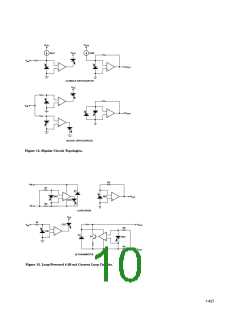
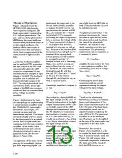
The 4-20 mA transmitter circuit in
Figure 15b is a little different
from the previous circuits, partic-
ularly the output circuit. The
output circuit does not directly
generate an output voltage which
is sensed by R2, it instead uses
Q1 to generate an output current
which flows through R3. This
output current generates a
voltage across R3, which is then
sensed by R2. An analysis similar
to the one above yields the
following expression relating
output current to input voltage:
The circuit operates in the same
way as the others. The only major
differences are the two compensa-
tion capacitors and additional
LED drive circuitry. In the high-
speed circuit discussed above, the
input and output circuits are
stabilized by reducing the local
loop gains of the input and output
circuits. Because reducing the
loop gains would decrease the
accuracy of the circuit, two
compensation capacitors, C1 and
C2, are instead used to improve
circuit stability. These capacitors
also limit the bandwidth of the
circuit to about 10 kHz and can
be used to reduce the output
noise of the circuit by reducing its
bandwidth even further.
bandwidth and gain stability at
low cost.
ILOOP/V = K*(R2+R3)/(R1*R3).
IN
To get into a little more detail
about the circuit, R1 is selected to
achieve an LED current of about
7-10 mA at the nominal input
operating voltage according to the
following equation:
The preceding circuits were pre-
sented to illustrate the flexibility
in designing analog isolation
circuits using the HCNR200/201.
The next section presents several
complete schematics to illustrate
practical applications of the
HCNR200/201.
IF = (VIN/R1)/K1,
where K1 (i.e., IPD1/IF) of the
optocoupler is typically about
0.5%. R2 is then selected to
achieve the desired output voltage
according to the equation,
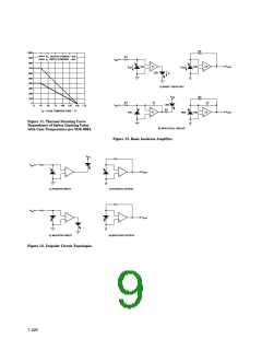
Example Application
Circuits
The circuit shown in Figure 16 is
a high-speed low-cost circuit
designed for use in the feedback
path of switch-mode power
The additional LED drive circuitry
(Q1 and R3 through R6) helps to
maintain the accuracy and band-
width of the circuit over the entire
range of input voltages. Without
these components, the transcon-
ductance of the LED driver would
VOUT/V = R2/R1.
IN
1-432

 AGILENT [ AGILENT TECHNOLOGIES, LTD. ]