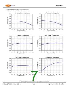
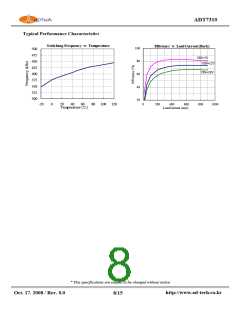
ADT7310
PCB design for optimized thermal performance
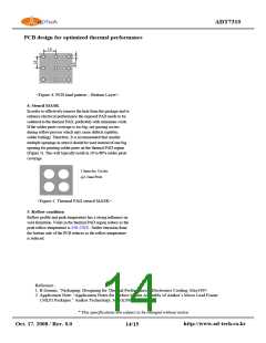
<Figure 4. PCB land pattern – Bottom Layer>
4. Stencil MASK
In order to effectively remove the heat from the package and to
enhance electrical performance the exposed PAD needs to be
soldered to the thermal PAD, preferably with minimum voids.
If the solder paste coverage is too big, out gassing occurs
during reflow process which may cause defects (splatter,
solder balling). Therefore, It is recommended that smaller
multiple openings in stencil should be used instead of one big
opening for printing solder paste on the thermal PAD region
(Figure 5). This will typically result in 50 to 80% solder paste
coverage
1.0mm dia. Circles
@1.2mm Pitch
<Figure 5. Thermal PAD stencil MASK>
5. Reflow condition
Reflow profile and peak temperature has a strong influence on
void formation. Voids in the thermal PAD region reduce as the
peak reflow temperature is 250~270℃. Solder extrusion from
the bottom side of the PCB reduces as the reflow temperature
is reduced.
Reference :
1. B.Guenin, “Packaging: Designing for Thermal Performance.” Electronics Cooling, May1997.
2. Application Note: “Application Notes for Surface Mount Assembly of Amkor’s Micro Lead Frame
( MLF) Packages.” Amkor Technology, March2001
* This specifications are subject to be changed without notice
http://www.ad-tech.co.kr
Oct. 17. 2008 / Rev. 0.0
14/15

 ADTECH [ ADTECH ]