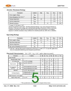
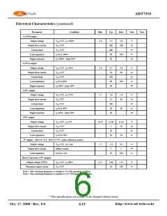
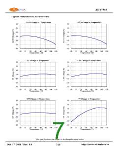
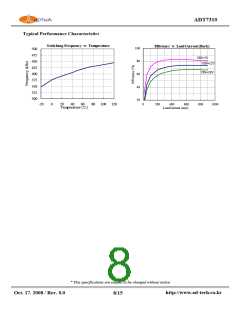
ADT7310
Operation Description
Note that external resistors for tuning negative voltage output
required as accurate as possible. It is recommended 1% accur-
acy. Because -7V output is generated by two cascaded charge
pump converter, this channel has operating voltage limitation.
With the operation above -7.5V, it is saturated and its regulati-
on performance degraded.
DEVICE INFORMATION
The ADT7310 includes one step down DC-DC switching buck
converter, one step up DC-DC switching boost converter, cha-
rge pump boost converter, charge pump inverting converter,
and several LDOs.
Especially produced for powering CCD camera applications,
this device provides various power channels for composing the
CCD applied camera system. These channel are 3.3V, 5V, 15V
, -7V and 1.8V. From these channel, it is possible to supply
all the powers required for the application in one power supply
device, ADT7310.
+15V channel is generated with two cascaded charge pump co-
nverters and one LDO. This channel output supplied current to
CCD device. So, its channel output noise affects image to noi-
se directly. This is why one LDO is added and therefore the
ADT7310 provides clear +15V output to the system.
The ADT7310 is assembled with small size and thermally enh-
anced MLF (Micro Lead Frame) package.
LDO
This device has four LDOs integrated (+3.3V 2 channel, +15V
and +1.8V channel). Because the ADT7310 provided for using
CCD camera application, the noise of each channel output mu-
st be minimized. Integration of LDOs trade off noiseless output
and heat dissipation performance of the device. From these
aspect, each channel load capability and input-output dropout
conditions are designed. By these considerations this device
provides optimum application function. Note that the heavy
load current and high line voltage application will produce the-
mal constraint.
With wide input operating voltage range and one stop power
supply configuration, it is very easy to design new specific set.
BUCK CONVERTER
Buck converter generates internal supply voltage (approxima-
tely 3.7V). As required wide input supply range from 4.75V to
18V, intermediate power is needed. From this intermediate
power all the channel outputs re-generated. Using a current
mode architecture with asynchronous rectification, the buck
converter have the ability to deliver sufficient current to the
following power supply channels.
POWER ON SEQUENCE
CCD camera application made by various devices requires ma-
ny different supply voltages. Also with different operating rati-
ng between devices, it is seriously considered to power up se-
quence. Fortunately CCD camera application has only two cri-
tical power supplies, +15V and -7V for powering the CCD.
Power on sequence that the system needs is as follows :
i) the -7V must be supplied lastly.
BOOST CONVERTER
5V output channel is generated by the boost converter. Operat-
ing with current mode step-up DC-DC converter, its input volt-
age is buck converter output voltage (3.7V typical). With this
boost converter output, supplied the power at the following
charge pump converters for generating +15V and -7V output.
Also it is provided +5V output with 100mA load current inde-
pendently. In case of upper 100mA load, must be considered
the device’s heat dissipation constraint.
ii) the +15V must be supplied before the -7V.
iii) other power supplies have no order.
Followed by the upper sequence, the ADT7310 operate succe-
ssfully when it is powered up. Further the ADT7310 will mon-
itor +3.3V channel voltage and generate RBO signal to reset
the DSP device. This RBO signal also follows after the -7V
channel settling.
CHARGE PUMP CONVERTER
By these converters the ADT7310 provides +15V and -7V cha-
nnel outputs. For these two channel generation, it is used three
charge pump converters, one with externally composed and
others with integrated. In case of generating charge pump inve-
rter the part of the inverter are placed at the outside of the devi-
ce for its inherent limitation of negative voltage operation. -7V
inverter is possible to change its output voltage by tuning the
external resistors.
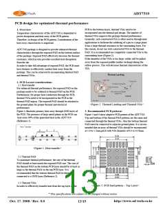
VIN
-7V
+15V
RBO
* This specifications are subject to be changed without notice
http://www.ad-tech.co.kr
Oct. 17. 2008 / Rev. 0.0
9/15

 ADTECH [ ADTECH ]