ADT7310
Application Hints (continued)
where IOUTMAX : maximum load current
OUTPUT CAPACITOR SELECTION
L : min. inductor value including worst case tolerance
Use a 10uF, 10V ceramic capacitor. Use X7R or X5R types,
do not use Y5V.
The output filter capacitor smoothes out current flow from the
inductor to the load, helps maintain a steady output voltage du-
ring transient load changes and reduces output voltage ripple.
These capacitors must be selected with sufficient capacitance
and sufficiently low ESR to perform these functions.
The output voltage ripple is caused by the charging and disch-
arging of the output capacitor and also due to its ESR and can
be calculated as :
CHARGE PUMP CONSIDERATIONS
DOUBLER / INVERTER CAPACITOR SELECTION
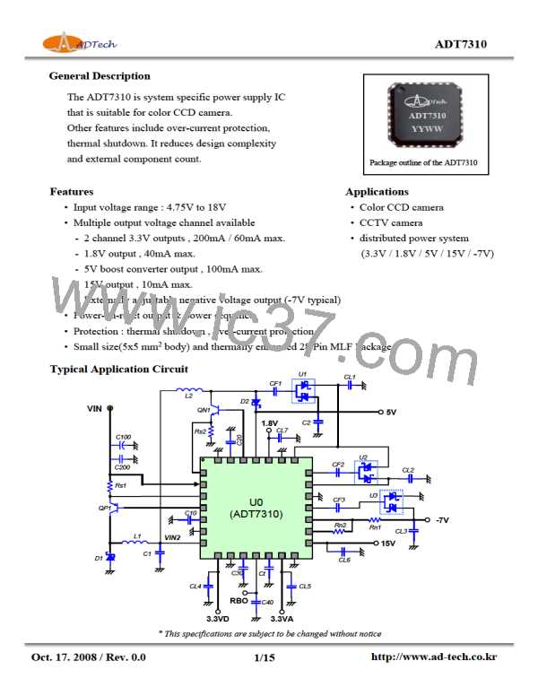
The flying capacitor (CF*) transfers charge from the its input
power supply to the output. A polarized capacitor (tantalum,
aluminum electrolytic, etc.) must not be used here, as the
capacitor will be reverse biased upon start-up of the ADT7310.
The size of the flying capacitor and its ESR affect output cur-
rent capability and ripple characteristic. In this applications,
a 1uF, X7R or X5R type ceramic capacitor is recommended
for the flying capacitor.
Voltage peak-to-peak ripple due to capacitance can be express-
ed as follows
VPP-C = IRIPPLE / (4 * f * C)
where IRIPPLE : Average to peak inductor current
f : Minimum switching frequency
The load capacitor (CL1,2,3) of the charge pump plays an imp-
ortant part in determining the characteristics of the doubler
output. The ESR of the output load capacitor affects charge
pump output resistance, which plays a role in determining
output current capability. Both output capacitance and ESR
affect output voltage ripple. For these reasons, a low value
ESR capacitor is recommended.
Voltage peak-to-peak ripple due to ESR can be expressed as
follows
VPP-ESR = (2 * IRIPPLE) * RESR
Because these two components are out of phase the rms value
can be used to get an approximate value of peak-to-peak
ripple.
Voltage peak-to-peak ripple, root mean squared can be expre-
ssed as follows
BOOST CONSIDERATIONS
2
V
PP-RMS = √ (VPP-C2 + VPP-ESR
)
Note that the output voltage ripple is dependent on the inductor
current ripple and the ESR of the output capacitor. The ESR
is frequency dependent (as well as temperature dependent),
make sure the value used for calculations is at the switching
frequency of the part.
INDUCTOR SELECTION
As previously mentioned from the inductor selection at the
buck converter, inductor at the boost converter also needs to be
considered two factors when choosing an inductor;
the inductor should not saturate, and the inductor current ripple
is small enough to achieve the desired output voltage ripple.
By the property of cascading boost converter from buck conv-
erter, its inductor saturation current is lower than the that of the
buck converter. In this application, the same 47uH adopted and
is sufficient. Boost converter drives both its load current and
the following charge pump converters for generating +15V and
-7V. For proper operation at the power up time this inductor
needs more saturation current than its total load current requir-
ed.
INPUT CAPACITOR SELECTION
The ADT7310 uses 10uF, 25V tantalum capacitor for input
capacitor. Use a mix of input bypass capacitors to control the
voltage overshoot. Use ceramic capacitor for the high frequen-
cy decoupling and tantalum capacitor to supply the required
rms input current. Place the input capacitor as close as possible
to the VIN pin of the device. The input filter capacitor supplies
current to the PNP switching transistor of the converter in the
first half of each cycle and reduces voltage ripple imposed on
the input power source. The input current ripple can be calcul-
ated as :
OUTPUT CAPACITOR SELECTION
VOUT VOUT r2
⎛
⎞
Use a 10uF, 10V ceramic capacitor. Use X7R or X5R types,
do not use Y5V. (the same component as buck converter)
⎜
⎟
IRMS = IOUTMAX ∗ 1−
∗
+
⎜
⎟
V
V
12
IN
⎝
IN
⎠
(VIN − VOUT )∗VOUT
r =
L∗f ∗IOUTMAX ∗V
IN
* This specifications are subject to be changed without notice
http://www.ad-tech.co.kr
Oct. 17. 2008 / Rev. 0.0
11/15

 ADTECH [ ADTECH ]