ADV7180
CGMS_WSS_AVL, CGMS/WSS Available, Address 0x78 [2],
User Sub Map, Read Only
CGMS and WSS
The CGMS and WSS data packets convey the same type of
information for different video standards. WSS is for PAL and
CGMS is for NTSC, so the CGMS and WSS readback registers
are shared. WSS is biphase coded; the VDP does a biphase
decoding to produce the 14 raw WSS bits in the CGMS/WSS
readback I2C registers and to set the CGMS_WSS_AVL bit.
0—CGMS/WSS was not detected.
1—CGMS/WSS was detected.
CGMS_WSS_DATA_0[3:0], Address 0x7D [3:0];
CGMS_WSS_DATA_1[7:0], Address 0x7E [7:0];
CGMS_WSS_DATA_2[7:0], Address 0x7F [7:0];
User Sub Map, Read Only
CGMS_WSS_CLEAR, CGMS/WSS Clear, Address 0x78 [2],
User Sub Map, Write Only, Self-Clearing
These bits hold the decoded CGMS or WSS data.
1—Reinitializes the CGMS/WSS readback registers.
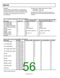
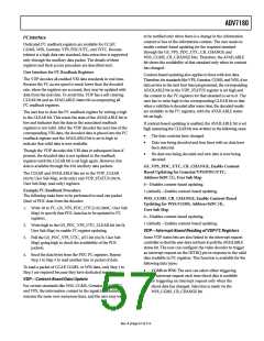
Refer to Figure 43 and Figure 44 for the I2C to WSS and CGMS
bit mapping.
VDP_CGMS_WSS_
VDP_CGMS_WSS_DATA_2 DATA_1[5:0]
0
1
2
3
4
5
6
7
0
1
2
3
4
5
RUN-IN
SEQUENCE
START
CODE
ACTIVE
VIDEO
11.0µs
38.4µs
42.5µs
Figure 43. WSS Waveform
+100 IRE
+70 IRE
VDP_CGMS_WSS_
DATA_0[3:0]
REF
VDP_CGMS_WSS_DATA_2
VDP_CGMS_WSS_DATA_1
0
1
2
3
4
5
6
7
0
1
2
3
4
5
6
7
0
1
2
3
0 IRE
49.1µs ± 0.5µs
–40 IRE
11.2µs
CRC SEQUENCE
2.235µs ± 20ns
Figure 44. CGMS Waveform
Table 77. CGMS Readback Registers1
Signal Name
Register Location
Address (User Sub Map)
CGMS_WSS_DATA_0[3:0]
CGMS_WSS_DATA_1[7:0]
CGMS_WSS_DATA_2[7:0]
VDP_CGMS_WSS_DATA_0[3:0]
VDP_CGMS_WSS_DATA_1[7:0]
VDP_CGMS_WSS_DATA_2[7:0]
125
126
127
0x7D
0x7E
0x7F
1 The register is a readback register; default value does not apply.
Rev. A | Page 60 of 112

 ADI [ ADI ]