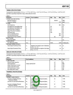
ADV7180
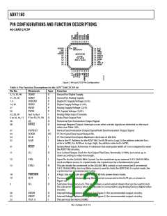
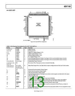
64-LEAD LQFP
64 63 62 61 60 59 58 57 56 55 54 53 52 51 50 49
1
2
48
47
46
45
44
43
42
41
40
39
38
37
36
35
34
33
INTRQ
HS
A
A
A
5
4
3
IN
IN
IN
PIN 1
3
DGND
DVDDIO
P11
4
NC
NC
5
6
P10
AGND
NC
ADV7180
7
P9
LQFP
TOP VIEW
(Not to Scale)
8
P8
NC
9
SFL
AVDD
VREFN
VREFP
AGND
10
11
12
13
14
15
16
DGND
DVDDIO
GPO1
GPO0
P7
A
A
2
1
IN
IN
P6
TEST_0
NC
P5
17 18 19 20 21 22 23 24 25 26 27 28 29 30 31 32
NC = NO CONNECT
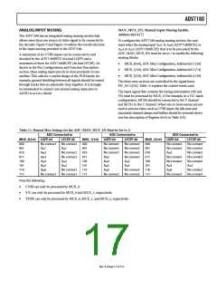
Figure 8. 64-Lead LQFP Pin Configuration
Table 9. Pin Function Description for the ADV7180 LQFP-64
Pin No.
Mnemonic
Type Function
3, 10, 24, 57
32, 37, 43
4, 11
23, 58
40
31
38
39
DGND
AGND
DVDDIO
DVDD
AVDD
PVDD
VREFP
VREFN
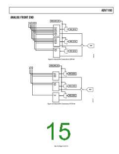
AIN1 to AIN6
G
G
P
P
P
P
O
O
I
Digital Ground.
Analog Ground.
Digital I/O Supply Voltage (3.3 V).
Digital Supply Voltage (1.8 V).
Analog Supply Voltage (1.8 V).
PLL Supply Voltage (1.8 V).
Internal Voltage Reference Output. See Figure 54 for recommended output circuitry.
Internal Voltage Reference Output. See Figure 54 for recommended output circuitry.
Analog Video Input Channels.
35, 36, 46 to 49
27, 28, 33, 41, 42,
44, 45, 50
NC
No Connect Pins. These pins are not connected internally.
5 to 8, 14 to 19,
25, 26, 59 to 62
P11 to P8,
P7 to P2, P1,
O
Video Pixel Output Port. See Table 96 for output configuration for 8-bit and 16-bit modes.
P0, P15 to P12
2
HS
VS
FIELD
INTRQ
O
O
O
O
Horizontal Synchronization Output Signal.
Vertical Synchronization Output Signal.
Field Synchronization Output Signal.
Interrupt Request Output. Interrupt occurs when certain signals are detected on the input
video (see Table 104).
I2C Port Serial Data Input/Output Pin.
I2C Port Serial Clock Input. Maximum clock rate of 400 kHz.
This pin selects the I2C address for the ADV7180. For ALSB set to Logic 0, the address
selected for a write is 0x40; for ALSB set to logic high, the address selected is 0x42.
64
63
1
53
54
52
SDATA
SCLK
ALSB
I/O
I
I
29
30
PWRDWN
ELPF
I
I
A logic low on this pin places the ADV7180 in power-down mode.
The recommended external loop filter must be connected to the ELPF pin, as shown in
Figure 54.
51
RESET
I
System Reset Input. Active low. A minimum low reset pulse width of 5 ms is required to reset
the ADV7180 circuitry.
Rev. A | Page 13 of 113

 ADI [ ADI ]