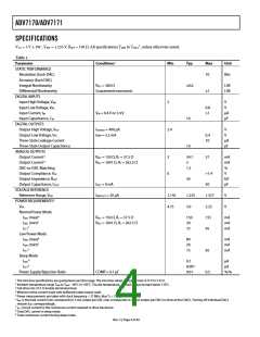
ADV7170/ADV7171
VAA = 3.0 V to 3.6 V1, VREF = 1.235 V, RSET = 150 Ω. All specifications TMIN to TMAX2, unless otherwise noted.
Table 6.
Parameter
MPU PORT3, 4
Conditions
Min Typ Max Unit
SCLOCK Frequency
0
400
kHz
μs
μs
μs
μs
ns
ns
ns
μs
SCLOCK High Pulse Width, t1
SCLOCK Low Pulse Width, t2
Hold Time (Start Condition), t3
Setup Time (Start Condition), t4
Data Setup Time, t5
SDATA, SCLOCK Rise Time, t6
SDATA, SCLOCK Fall Time, t7
Setup Time (Stop Condition), t8
ANALOG OUTPUTS3, 5
Analog Output Delay
DAC Analog Output Skew
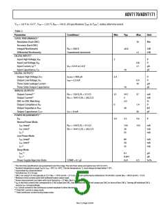
CLOCK CONTROLAND PIXEL PORT4, 5, 6
fCLOCK
0.6
1.3
0.6
0.6
100
After this period the first clock is generated
Relevant for repeated start condition
300
300
0.6
7
0
ns
ns
27
MHz
Clock High Time, t9
8
ns
Clock Low Time, t10
8
ns
Data Setup Time, t11
Data Hold Time, t12
3.5
4
ns
ns
Control Setup Time, t11
Control Hold Time, t12
Digital Output Access Time, t13
Digital Output Hold Time, t14
Pipeline Delay, t15
4
3
ns
ns
ns
ns
12
8
48
Clock cycles
TELETEXT3, 4, 7
Digital Output Access Time, t16
Data Setup Time, t17
Data Hold Time, t18
23
2
6
ns
ns
ns
RESET CONTROL3, 4
Low Time
6
ns
RESET
1 The max/min specifications are guaranteed over this range. The max/min values are typical over 3.0 V to 3.6 V range.
2 Ambient temperature range TMIN to TMAX: −40°C to +85°C. The die temperature, TJ, must always be kept below 110°C.
3 TTL input values are 0 V to 3 V, with input rise/fall times ≤3 ns, measured between the 10% and 90% points. Timing reference points at 50% for inputs and outputs.
Analog output load ≤10 pF.
4 Guaranteed by characterization
5 Output delay measured from the 50% point of the rising edge of CLOCK to the 50% point of full-scale transition
6 Pixel Port consists of the following:
Pixel inputs:
Pixel controls:
Clock input:
P15–P0
HSYNC
VSYNC BLANK
, FIELD/
,
CLOCK
7 Teletext port consists of the following:
Teletext output: TTXREQ
Teletext input: TTX
Rev. C | Page 8 of 64

 ADI [ ADI ]