ADV7170/ADV7171
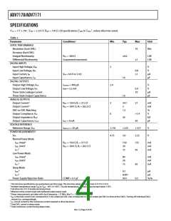
VAA = 3.0 V to 3.6 V1, VREF = 1.235 V, RSET = 150 Ω. All specifications TMIN to TMAX2, unless otherwise noted.
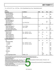
Table 2.
Parameter
Conditions1
Min
Typ
Max
Unit
STATIC PERFORMANCE3
Resolution (Each DAC)
Accuracy (Each DAC)
Integral Nonlinearity
Differential Nonlinearity
DIGITAL INPUTS3
10
Bits
RSET = 300 Ω
Guaranteed monotonic
0.6
LSB
LSB
1
Input High Voltage, VINH
Input Low Voltage, VINL
Input Current, IIN
Input Capacitance, CIN
DIGITAL OUTPUTS3
2
V
V
μA
pF
0.8
1
3, 4
VIN = 0.4 V or 2.4 V
10
10
Output High Voltage, VOH
Output Low Voltage, VOL
Three-State Leakage Current
Three-State Output Capacitance
ANALOG OUTPUTS3
Output Current4, 5
ISOURCE = 400 μA
ISINK = 3.2 mA
2.4
V
V
μA
pF
0.4
10
RSET = 150 Ω, RL = 37.5 Ω
RSET = 1041 Ω, RL = 262.5 Ω
33
0
34.7
5
2.0
37
mA
mA
%
V
kΩ
pF
Output Current6
DAC-to-DAC Matching
Output Compliance, VOC
Output Impedance, ROUT
Output Capacitance, COUT
POWER REQUIREMENTS3, 7
VAA
1.4
30
30
IOUT = 0 mA
3.0
3.3
3.6
155
V
Normal Power Mode
IDAC (max)8
RSET = 150 Ω, RL = 37.5 Ω
RSET = 1041 Ω, RL = 262.5 Ω
150
20
35
mA
mA
mA
IDAC (min)8
9
ICCT
Low Power Mode
IDAC (max)8
80
20
35
mA
mA
mA
IDAC (min)8
9
ICCT
Sleep Mode
10
IDAC
ICCT
0.1
0.001
0.01
μA
μA
%/%
11
Power Supply Rejection Ratio
COMP = 0.1 μF
0.5
1 The min/max specifications are guaranteed over this range. The min/max values are typical over 3.0 V to 3.6 V.
2 Ambient temperature range TMIN to TMAX: −40°C to +85°C. The die temperature, TJ, must always be kept below 110°C.
3 Guaranteed by characterization.
4 Full drive into 37.5 Ω load.
5 DACs can output 35 mA typically at 3.3 V (RSET = 150 Ω and RL = 37.5 Ω); optimum performance obtained at 18 mA DAC current (RSET = 300 Ω and RL = 75 Ω).
6 Minimum drive current (used with buffered/scaled output load).
7 Power measurements are taken with clock frequency = 27 MHz. Max TJ = 110°C.
8 IDAC is the total current (min corresponds to 5 mA output per DAC, max corresponds to 38 mA output per DAC) to drive all four DACs. Turning off individual DACs
reduces IDAC correspondingly.
9 ICCT (circuit current) is the continuous current required to drive the device.
10 Total DAC current in sleep mode.
11 Total continuous current during sleep mode.
Rev. C | Page 5 of 64

 ADI [ ADI ]