ADSP-21062/ADSP-21062L
ADSP-21000 FAMILY CORE ARCHITECTURE
Instruction Cache
The ADSP-21062 includes the following architectural features
of the ADSP-21000 family core. The ADSP-21062 processors
are code- and function-compatible with the ADSP-21020.
The ADSP-21062 includes an on-chip instruction cache that
enables three-bus operation for fetching an instruction and two
data values. The cache is selective—only the instructions whose
fetches conflict with PM bus data accesses are cached. This
allows full-speed execution of core, looped operations such as
digital filter multiply-accumulates and FFT butterfly processing.
Independent, Parallel Computation Units
The arithmetic/logic unit (ALU), multiplier and shifter all per-
form single-cycle instructions. The three units are arranged in
parallel, maximizing computational throughput. Single multi-
function instructions execute parallel ALU and multiplier opera-
tions. These computation units support IEEE 32-bit single-
precision floating-point, extended precision 40-bit floating-
point, and 32-bit fixed-point data formats.
Data Address Generators with Hardware Circular Buffers
The ADSP-21062’s two data address generators (DAGs) imple-
ment circular data buffers in hardware. Circular buffers allow
efficient programming of delay lines and other data structures
required in digital signal processing, and are commonly used in
digital filters and Fourier transforms. The two DAGs of the
ADSP-21062 contain sufficient registers to allow the creation of
up to 32 circular buffers (16 primary register sets, 16 secondary).
The DAGs automatically handle address pointer wraparound,
reducing overhead, increasing performance and simplifying
implementation. Circular buffers can start and end at any
memory location.
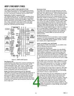
ADSP-2106x
BMS
1x CLOCK
3
CLKIN
EBOOT
LBOOT
CS
BOOT
EPROM
(OPTIONAL)
ADDR
DATA
IRQ
2-0
FLAG
3-0
TIMEXP
4
ADDR
ADDR
DATA
31-0
MEMORY
AND
PERIPHERALS
(OPTIONAL)
DATA
47-0
Flexible Instruction Set
LINK
DEVICES
(6 MAXIMUM)
(OPTIONAL)
LxCLK
LxACK
LxDAT
3-0
RD
WR
OE
WE
The 48-bit instruction word accommodates a variety of parallel
operations, for concise programming. For example, the ADSP-
21062 can conditionally execute a multiply, an add, a subtract
and a branch, all in a single instruction.
ACK
ACK
CS
MS
3-0
TCLK0
RCLK0
TFS0
RSF0
DT0
PAGE
SBTS
SW
SERIAL
DEVICE
(OPTIONAL)
DMA DEVICE
(OPTIONAL)
DATA
ADSP-21062/ADSP-21062L FEATURES
Augmenting the ADSP-21000 family core, the ADSP-21062
adds the following architectural features:
ADRCLK
DMAR1-2
DMAG1-2
DR0
TCLK1
RCLK1
TFS1
RFS1
DT1
CS
HBR
Dual-Ported On-Chip Memory
SERIAL
DEVICE
(OPTIONAL)
HOST
PROCESSOR
INTERFACE
(OPTIONAL)
The ADSP-21062 contains two megabits of on-chip SRAM,
organized as two blocks of 1 Mbits each, which can be config-
ured for different combinations of code and data storage. Each
memory block is dual-ported for single-cycle, independent ac-
cesses by the core processor and I/O processor or DMA control-
ler. The dual-ported memory and separate on-chip buses allow
two data transfers from the core and one from I/O, all in a single
cycle.
HBG
REDY
DR1
BR
1-6
ADDR
DATA
RPBA
CPA
JTAG
ID
2-0
RESET
7
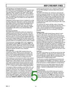
Figure 2. ADSP-21062 System
Data Register File
On the ADSP-21062, the memory can be configured as a maxi-
mum of 64K words of 32-bit data, 128K words of 16-bit data,
40K words of 48-bit instructions (or 40-bit data), or combina-
tions of different word sizes up to two megabits. All of the
memory can be accessed as 16-bit, 32-bit or 48-bit words.
A general purpose data register file is used for transferring data
between the computation units and the data buses, and for
storing intermediate results. This 10-port, 32-register (16 pri-
mary, 16 secondary) register file, combined with the ADSP-
21000 Harvard architecture, allows unconstrained data flow
between computation units and internal memory.
A 16-bit floating-point storage format is supported, which effec-
tively doubles the amount of data that may be stored on-chip.
Conversion between the 32-bit floating-point and 16-bit floating-
point formats is done in a single instruction.
Single-Cycle Fetch of Instruction and Two Operands
The ADSP-21062 features an enhanced Harvard architecture in
which the data memory (DM) bus transfers data and the pro-
gram memory (PM) bus transfers both instructions and data
(see Figure 1). With its separate program and data memory
buses and on-chip instruction cache, the processor can simulta-
neously fetch two operands and an instruction (from the cache),
all in a single cycle.
While each memory block can store combinations of code and
data, accesses are most efficient when one block stores data,
using the DM bus for transfers, and the other block stores
instructions and data, using the PM bus for transfers. Using the
DM bus and PM bus in this way, with one dedicated to each
memory block, assures single-cycle execution with two data
transfers. In this case, the instruction must be available in the
cache. Single-cycle execution is also maintained when one of the
data operands is transferred to or from off-chip, via the ADSP-
21062’s external port.
REV. C
–4–

 ADI [ ADI ]