ADSP-21062/ADSP-21062L
DMA Controller
Multiprocessing
10 DMA Channels for Transfers Between ADSP-21062
Internal Memory and External Memory, External
Peripherals, Host Processor, Serial Ports, or Link
Ports
Background DMA Transfers at 40 MHz, in Parallel with
Full-Speed Processor Execution
Glueless Connection for Scalable DSP Multiprocessing
Architecture
Distributed On-Chip Bus Arbitration for Parallel Bus
Connect of Up to Six ADSP-21062s Plus Host
Six Link Ports for Point-to-Point Connectivity and Array
Multiprocessing
240 Mbytes/s Transfer Rate Over Parallel Bus
240 Mbytes/s Transfer Rate Over Link Ports
Host Processor Interface to 16- and 32-Bit Microprocessors
Host Can Directly Read/Write ADSP-21062 Internal
Memory
Serial Ports
Two 40 Mbit/s Synchronous Serial Ports with Com-
panding Hardware
Independent Transmit and Receive Functions
Figure 7. JTAG Clocktree for Multiple ADSP-2106x
TABLE OF CONTENTS
Systems . . . . . . . . . . . . . . . . . . . . . . . . . . . . . . . . . . . . . . 12
Figure 8. Clock Input . . . . . . . . . . . . . . . . . . . . . . . . . . . . . 18
Figure 9. Reset . . . . . . . . . . . . . . . . . . . . . . . . . . . . . . . . . . 18
Figure 10. Interrupts . . . . . . . . . . . . . . . . . . . . . . . . . . . . . . 18
Figure 11. Timer . . . . . . . . . . . . . . . . . . . . . . . . . . . . . . . . 19
Figure 12. Flags . . . . . . . . . . . . . . . . . . . . . . . . . . . . . . . . . 19
Figure 13. Memory Read—Bus Master . . . . . . . . . . . . . . . . 20
Figure 14. Memory Write—Bus Master . . . . . . . . . . . . . . . 21
Figure 15. Synchronous Read/Write—Bus Master . . . . . . . 23
Figure 16. Synchronous Read/Write—Bus Slave . . . . . . . . . 25
Figure 17. Multiprocessor Bus Request and Host Bus
GENERAL DESCRIPTION . . . . . . . . . . . . . . . . . . . . . . . . . 3
ADSP-21000 FAMILY CORE ARCHITECTURE . . . . . . . 4
ADSP-21062/ADSP-21062L FEATURES . . . . . . . . . . . . . . 4
DEVELOPMENT TOOLS . . . . . . . . . . . . . . . . . . . . . . . . . . 7
PIN FUNCTION DESCRIPTIONS . . . . . . . . . . . . . . . . . . 8
TARGET BOARD CONNECTOR FOR EZ-ICE®
PROBE . . . . . . . . . . . . . . . . . . . . . . . . . . . . . . . . . . . . . . 11
RECOMMENDED OPERATING CONDITIONS . . . . . . 13
ELECTRICAL CHARACTERISTICS . . . . . . . . . . . . . . . . 13
TIMING SPECIFICATIONS . . . . . . . . . . . . . . . . . . . . . . . 17
Memory Read—Bus Master . . . . . . . . . . . . . . . . . . . . . . . 20
Memory Write—Bus Master . . . . . . . . . . . . . . . . . . . . . . 21
Synchronous Read/Write—Bus Master . . . . . . . . . . . . . . 22
Synchronous Read/Write—Bus Slave . . . . . . . . . . . . . . . . 24
Multiprocessor Bus Request and Host Bus Request . . . . . 26
Asynchronous Read/Write—Host to ADSP-21062 . . . . . . 28
Three-State Timing—Bus Master, Bus Slave,
HBR, SBTS . . . . . . . . . . . . . . . . . . . . . . . . . . . . . . . . . 30
DMA Handshake . . . . . . . . . . . . . . . . . . . . . . . . . . . . . . . 31
Link Ports: 1 × CLK Speed Operation . . . . . . . . . . . . . . 33
Link Ports: 2 × CLK Speed Operation . . . . . . . . . . . . . . 34
Serial Ports . . . . . . . . . . . . . . . . . . . . . . . . . . . . . . . . . . . . 36
JTAG Test Access Port and Emulation . . . . . . . . . . . . . . . 39
OUTPUT DRIVE CURRENTS . . . . . . . . . . . . . . . . . . . . . 40
POWER DISSIPATION . . . . . . . . . . . . . . . . . . . . . . . . . . . 40
TEST CONDITIONS . . . . . . . . . . . . . . . . . . . . . . . . . . . . 40
ENVIRONMENTAL CONDITIONS . . . . . . . . . . . . . . . . 43
225 Ball Plastic Ball Grid Array (PBGA)
Request . . . . . . . . . . . . . . . . . . . . . . . . . . . . . . . . . . . . . . 27
Figure 18a. Synchronous REDY Timing . . . . . . . . . . . . . . 28
Figure 18b. Asynchronous Read/Write—Host to
ADSP-21062 . . . . . . . . . . . . . . . . . . . . . . . . . . . . . . . . . . 29
Figure 19a. Three-State Timing (Bus Transition Cycle,
SBTS Assertion) . . . . . . . . . . . . . . . . . . . . . . . . . . . . . . . 30
Figure 19b. Three-State Timing (Host Transition Cycle) . . 30
Figure 20. DMA Handshake Timing . . . . . . . . . . . . . . . . . 32
Figure 21. Link Ports . . . . . . . . . . . . . . . . . . . . . . . . . . . . . 35
Figure 22. Serial Ports . . . . . . . . . . . . . . . . . . . . . . . . . . . . 37
Figure 23. External Late Frame Sync . . . . . . . . . . . . . . . . . 38
Figure 24. IEEE 11499.1 JTAG Test Access Port . . . . . . . 39
Figure 25. Output Enable/Disable . . . . . . . . . . . . . . . . . . . 41
Figure 26. Equivalent Device Loading for AC Measurements
(Includes All Fixtures) . . . . . . . . . . . . . . . . . . . . . . . . . . . 41
Figure 27. Voltage Reference Levels for AC Measurements
(Except Output Enable/Disable) . . . . . . . . . . . . . . . . . . . 41
Figure 28. ADSP-21062 Typical Drive Currents
Package Descriptions . . . . . . . . . . . . . . . . . . . . . . . . . 44
225 Ball Plastic Ball Grid Array (PBGA)
(VDD = 5 V) . . . . . . . . . . . . . . . . . . . . . . . . . . . . . . . . . . . 42
Figure 29. Typical Output Rise Time (10%–90% VDD
)
Package Pinout . . . . . . . . . . . . . . . . . . . . . . . . . . . . . . 45
PACKAGE DIMENSIONS, 225-Ball PBGA . . . . . . . . . . . 46
240-LEAD METRIC MQFP PIN CONFIGURATIONS . . 47
PACKAGE DIMENSIONS, 240-Lead Metric MQFP . . . 48
ORDERING GUIDE . . . . . . . . . . . . . . . . . . . . . . . . . . . . . 48
vs. Load Capacitance (VDD = 5 V) . . . . . . . . . . . . . . . . . . 42
Figure 30. Typical Output Rise Time (0.8 V–2.0 V) vs. Load
Capacitance (VDD = 5 V) . . . . . . . . . . . . . . . . . . . . . . . . . 42
Figure 31. Typical Output Delay or Hold vs. Load Capacitance
(at Maximum Case Temperature) (VDD = 5 V) . . . . . . . . 42
Figure 32. ADSP-21062 Typical Drive Currents
Figures
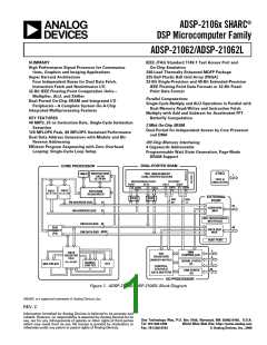
Figure 1. ADSP-21062/ADSP-21062L Block Diagram . . . . 1
Figure 2. ADSP-21062 System . . . . . . . . . . . . . . . . . . . . . . . 4
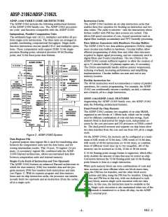
Figure 3. Shared Memory Multiprocessing System . . . . . . . . 6
Figure 4. ADSP-21062/ADSP-21062L Memory Map . . . . . 7
Figure 5. Target Board Connector For ADSP-2106x
EZ-ICE Emulator (Jumpers in Place) . . . . . . . . . . . . . . . 11
Figure 6. JTAG Scan Path Connections for Multiple
ADSP-2106x Systems . . . . . . . . . . . . . . . . . . . . . . . . . . . 11
(VDD = 3.3 V) . . . . . . . . . . . . . . . . . . . . . . . . . . . . . . . . . 42
Figure 33. Typical Output Rise Time (10%–90% VDD
)
vs. Load Capacitance (VDD = 3.3 V) . . . . . . . . . . . . . . . . 42
Figure 34. Typical Output Rise Time (0.8 V–2.0 V) vs. Load
Capacitance (VDD = 3.3 V) . . . . . . . . . . . . . . . . . . . . . . . 43
Figure 35. Typical Output Delay or Hold vs. Load Capacitance
(at Maximum Case Temperature) (VDD = 3.3 V) . . . . . . . 43
EZ-ICE is a registered trademark of Analog Devices, Inc.
REV. C
–2–

 ADI [ ADI ]