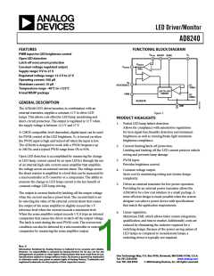
AD8240
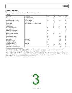
SPECIFICATIONS
TA = operating temperature range, VPLUS = 13.5 V, unless otherwise noted.
Table 1.
Parameter
Conditions
Min
Typ
12
1
Max
Unit
V
%
%
mA
µs
VO
5 V Reference = 5 V
VPLUS = 13 V to 27 V
VPLUS = 13 V to 27 V
RSHUNT = 0.4 Ω
VO Regulation1 at 25°C
VO Regulation2 -40°C to 125°C
−3
−6
+3
+6
2
3
IOUT
500
12
24
3
VO Rise Time
VSENSE Gain
VSENSE Accuracy
VSENSE Output Impedance
Base Drive
PWM Turn-On Threshold
PWM Turn-Off Threshold
VSENSE Latch-Off Threshold4
Latch-Off Delay5
PWM Frequency Range
CM
IOUT = 250 mA, CM = 22 nF, CL = 47 nF
−7
8
15
3.5
+7
12
%
10
kΩ
mA
V
V
V
µs
Hz
nF
%
µA
V
µA
µA
°C
1.4
0.3
0
0.1
2
DC
22
−30
500
CLOAD Range
CL = 47 nF
VPLUS > 13 V
+30
360
27
10
240
+125
Operating Current6
VPLUS Operating Range
Shutdown Current
5 V Reference Current
Operating Temperature Range
9
PWM low
160
−40
200
1 VO = 12/5 of the applied reference voltage 1% typical. Minimum VPLUS voltage for regulation depends on the external transistor Vbe and the shunt voltage.
2 VO = 12/5 of the applied reference voltage 2% typical. Minimum VPLUS voltage for regulation depends on the external transistor Vbe and the shunt voltage.
3 The maximum output current level is set by the selection of the current shunt and power transistor.
4 (VSENSE – 5 V Reference) The latch-off level is determined by the output level of the sense amplifier. When the amplifier output approaches 5 V, the output is latched off.
This allows the maximum current output level to be determined by the shunt resistor value. Latch-off can be restored to on by cycling the PWM input off and back on.
5 Internal delay only. The external delay depends on the external capacitor values, LED string impedance, and wiring inductance.
6 This specifies VPLUS only—ground current includes external transistor base drive.
Rev. 0 | Page 3 of 12

 ADI [ ADI ]