Data Sheet
AD7904/AD7914/AD7924
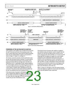
APPLICATIONS INFORMATION
The SPORT0 control register of the ADSP-218x should be set
up as follows:
MICROPROCESSOR INTERFACING
The serial interface of the AD7904/AD7914/AD7924 allows
the part to be directly connected to a range of different
microprocessors. This section explains how to interface the
AD7904/AD7914/AD7924 to some of the more common
microcontroller and DSP serial interface protocols.
TFSW = RFSW = 1, alternate framing
INVRFS = INVTFS = 1, active low frame signal
DTYPE = 00, right justify data
SLEN = 1111, 16-bit data-words
ISCLK = 1, internal serial clock
TFSR = RFSR = 1, frame every word
IRFS = 0
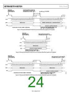
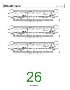
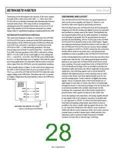
AD7904/AD7914/AD7924 to TMS320C541
The serial interface of the TMS320C541 uses a continuous serial
clock and frame synchronization signals to synchronize the data
transfer operations with peripheral devices such as the AD7904/
ITFS = 1
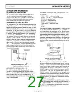
The connection diagram is shown in Figure 31. The ADSP-218x
has the TFS and RFS of the SPORT tied together, with TFS set
as an output and RFS set as an input. The DSP operates in alter-
nate framing mode and the SPORT0 control register is set up as
described. The frame synchronization signal generated on the
CS
AD7914/AD7924. The
input allows easy interfacing between
the TMS320C541 and the AD7904/AD7914/AD7924 without any
glue logic required. The serial port of the TMS320C541 is set up
to operate in burst mode with internal CLKX0 (TX serial clock
on Serial Port 0) and FSX0 (TX frame sync from Serial Port 0).
The serial port control (SPC) register must have the following
setup: FO = 0, FSM = 1, MCM = 1, and TXM = 1. The connection
diagram is shown in Figure 30. Note that for signal processing
applications, it is imperative that the frame synchronization
signal from the TMS320C541 provide equidistant sampling.
The VDRIVE pin of the AD7904/AD7914/AD7924 takes the same
supply voltage as the TMS320C541. This allows the ADC to
operate at a higher voltage than the serial interface, that is, the
TMS320C541, if necessary.
CS
TFS is tied to
and, as with all signal processing applications,
equidistant sampling is necessary. However, in this example, the
timer interrupt is used to control the sampling rate of the ADC,
and under certain conditions equidistant sampling may not be
achieved.
ADSP-218x*
AD7904/
AD7914/
AD7924*
SCLK
SCLK
DR
DOUT
CS
RFS
TFS
TMS320C541*
AD7904/
AD7914/
AD7924*
DIN
DT
V
DRIVE
SCLK
CLKX
CLKR
DOUT
DIN
DR
DT
V
DD
*ADDITIONAL PINS REMOVED FOR CLARITY.
CS
FSX
FSR
Figure 31. Interfacing to the ADSP-218x
V
DRIVE
The timer register, for example, is loaded with a value that
provides an interrupt at the required sample interval. When an
interrupt is received, a value is transmitted with TFS/DT (ADC
control word). The TFS is used to control the RFS and thus the
reading of data. The frequency of the serial clock is set in the
SCLKDIV register. When the instruction to transmit with TFS
is given (that is, AX0 = TX0), the state of the SCLK is checked.
The DSP waits until SCLK goes high, low, and high again before
transmission starts. If the timer and SCLK values are chosen in
such a way that the instruction to transmit occurs on or near
the rising edge of SCLK, the data may be transmitted or it may
wait until the next clock edge.
V
DD
*ADDITIONAL PINS REMOVED FOR CLARITY.
Figure 30. Interfacing to the TMS320C541
AD7904/AD7914/AD7924 to ADSP-218x
The ADSP-218x family of DSPs interfaces directly to the
AD7904/AD7914/AD7924 without any glue logic required.
The VDRIVE pin of the AD7904/AD7914/AD7924 takes the same
supply voltage as the ADSP-218x. This allows the ADC to
operate at a higher voltage than the serial interface, that is, the
ADSP-218x, if necessary.
For example, if the ADSP-2189 has a 20 MHz crystal so that its
master clock frequency is 40 MHz, then the master cycle time is
25 ns. If the SCLKDIV register is loaded with the value 3, then
an SCLK of 5 MHz is obtained and eight master clock periods
elapse for every one SCLK period.
Rev. C | Page 27 of 32

 ADI [ ADI ]