AD7715
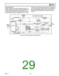
Smart Transmitters
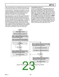
The AD7715 consumes only 450 µA, leaving 3 mA available for
the rest of the transmitter. Figure 15 shows a block diagram of a
smart transmitter which includes the AD7715. Not shown in
Figure 15 is the isolated power source required to power the
front end.
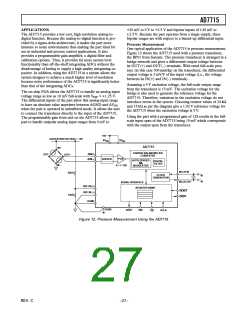
Another area where the low power, single supply, three-wire
interface capabilities is of benefit is in smart transmitters. Here,
the entire smart transmitter must operate from the 4 mA to
20 mA loop. Tolerances in the loop mean that the amount of
current available to power the transmitter is as low as 3.5 mA.
ISOLATION
BARRIER
MAIN TRANSMITTER ASSEMBLY
3V
ISOLATED SUPPLY
VOLTAGE
REGULATOR
VOLTAGE
VOLTAGE
REFERENCE
REFERENCE
V
CC
AV
DD
DV
DD
REF IN
INPUT/OUTPUT
D/A
CONVERTER
STAGE
MICROCONTROLLER UNIT
4–20mA
SIGNAL
SENSORS
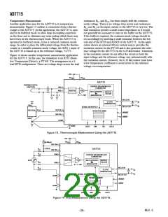
RTD
mV
ohm
CONDITIONER
*PID
LOOP
RTN
AD7715
MCLK
IN
*RANGE SETTING
*CALIBRATION
*LINEARIZATION
*OUTPUT CONTROL
*SERIAL COMMUNICATION
*HART PROTOCOL
COM
3V
TC
WAVEFORM
SHAPER
BANDPASS
FILTER
HART
MODEM
BELL 202
MCLK
OUT
AGND
ISOLATED GROUND
COM
DGND
Figure 15. Smart Transmitter Using the AD7715
REV. C
–29–

 ADI [ ADI ]