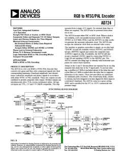
AD724
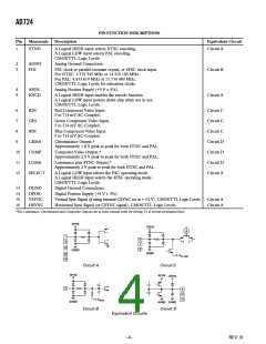
PIN FUNCTION DESCRIPTIONS
Pin
Mnemonic
Description
Equivalent Circuit
1
STND
A Logical HIGH input selects NTSC encoding.
A Logical LOW input selects PAL encoding.
CMOS/TTL Logic Levels.
Circuit A
2
3
AGND
FIN
Analog Ground Connection.
FSC clock or parallel-resonant crystal, or 4FSC clock input.
For NTSC: 3.579 545 MHz or 14.318 180 MHz.
For PAL: 4.433 619 MHz or 17.734 480 MHz.
CMOS/TTL Logic Levels for subcarrier clocks.
Circuit B
Circuit A
4
5
APOS
Analog Positive Supply (+5 V ± 5%).
ENCD
A Logical HIGH input enables the encode function.
A Logical LOW input powers down chip when not in use.
CMOS/TTL Logic Levels.
6
RIN
Red Component Video Input.
0 to 714 mV AC-Coupled.
Circuit C
Circuit C
Circuit C
Circuit D
Circuit D
Circuit D
Circuit A
7
GIN
Green Component Video Input.
0 to 714 mV AC-Coupled.
8
BIN
Blue Component Video Input.
0 to 714 mV AC-Coupled.
9
CRMA
COMP
LUMA
SELECT
Chrominance Output.*
Approximately 1.8 V peak-to-peak for both NTSC and PAL.
10
11
12
Composite Video Output.*
Approximately 2.5 V peak-to-peak for both NTSC and PAL.
Luminance plus SYNC Output.*
Approximately 2 V peak-to-peak for both NTSC and PAL.
A Logical LOW input selects the FSC operating mode.
A Logical HIGH input selects the 4FSC operating mode.
CMOS/TTL Logic Levels.
13
14
15
16
DGND
DPOS
Digital Ground Connections.
Digital Positive Supply (+5 V ± 5%).
VSYNC
HSYNC
Vertical Sync Signal (if using external CSYNC set at > +2 V). CMOS/TTL Logic Levels.
Horizontal Sync Signal (or CSYNC signal). CMOS/TTL Logic Levels.
Circuit A
Circuit A
*The Luminance, Chrominance and Composite Outputs are at twice normal levels for driving 75 Ω reverse-terminated lines.
DPOS
DPOS
1
6
5
7
12
8
DGND
DGND
15
16
V
CLAMP
Circuit A
Circuit C
DPOS
APOS
DPOS
3
9
10
11
V
BIAS
DGND
AGND DGND
Circuit B
Circuit D
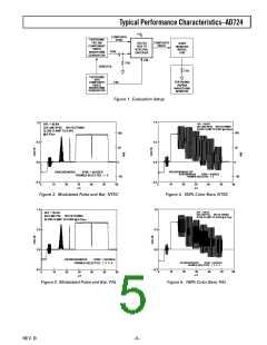
Equivalent Circuits
–4–
REV. B

 ADI [ ADI ]