AD5399
OPERATION
The AD5399 provides a 12-bit, twos complement, dual voltage
output, digital-to-analog converter (DAC). It has an internal
reference with 2 V bipolar zero dc offset, where ꢀ ≤ VOUT ≤ 4 V.
1kΩ
LOGIC
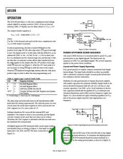
Figure 21. Equivalent ESD Protection Circuit
The output transfer equation is
5V
V
V
DD
V
OUT = ((D – 2ꢀ48)/4ꢀ96 × 4 V) + 2 V
C1
10µF
C2
0.1µF
TP
AD5399
V
)
OUTA
CS
where:
(D–2048)/4096 × 4V + 2V
V
(V
CLK
SDI
BZ REF
2V
D is the 12-bit decimal code and not the twos complement code.
OUT is with respect to ground.
DGND AGND
V
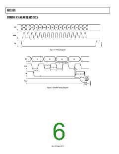
In data programming, the data is loaded MSB first on the
Figure 22. Basic Connection
positive clock edge (SCLK) after chip select ( ) goes from high
CS
POWER-UP/POWER-DOWN SEQUENCE
to low. The digital word is 16 bits wide, with the MSB, B15, as an
address bit (DAC A: Aꢀ = ꢀ; DAC B: Aꢀ = 1). B14 is don’t care,
B13 is a shutdown bit, B12 must be logic low, and the last 12 bits
are data bits. An internal counter allows data transferred from
the shift register to the output after the 16th positive clock edge
Like most CMOS devices, it is recommended to power VDD and
ground prior to any digital signals. The ideal power-up
sequence is GND, VDD, and digital signals. The reverse sequence
applies to the power-down condition.
while
stays low (see Figure 5). After the 16th clock pulse, it is
CS
Layout and Power Supply Bypassing
not necessary to bring
high to shift the data to the output.
CS
It is a good practice to employ compact, minimum lead-length
layout design. The input leads should be as direct as possible
with a minimum conductor length. Ground paths should have
low resistance and low inductance.
However, should be brought high anytime after the 16th clock
CS
positive edge in order to allow the next programming cycle.
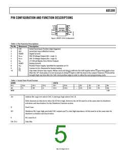
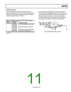
Table 6. Input Logic Control Truth Table
Similarly, it is also good practice to bypass the power supplies
with quality capacitors for optimum stability. Supply leads to the
device should be bypassed with ꢀ.ꢀ1 µF to ꢀ.1 µF disc or chip
ceramic capacitors. Low ESR 1 µF to 1ꢀ µF tantalum or electro-
lytic capacitors should also be applied at VDD to minimize any
transient disturbance and to filter any low frequency ripple (see
Figure 23). Users should not apply switching regulators for VDD
due to the power supply rejection ratio degradation over
frequency.
CLK
CS
Register Activity
L
H
P
16th
H
H
L
No Shift Register Effect
No Shift Register Effect
Shift One SDI Bit into the SR
Transfer SR Data into DAC Register and Update
the Output
P
L
P = Positive Edge, X = Don't Care, SR = Shift Register.
The data setup and data hold times in the Specifications table
determine the timing requirements. The internal power-on reset
circuit clears the serial input registers to all ꢀs, and sets the two
DAC registers to a VBZ (zero code) of 2 V.
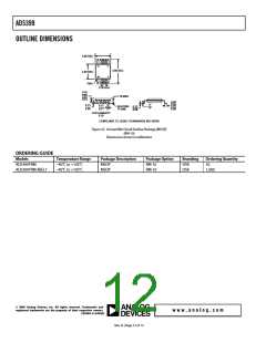
AD5399
V
V
DD
DD
+
C2
C1
Software shutdown B13 turns off the internal REF and
amplifiers. The output is close to zero potential, and the digital
circuitry remains active such that new data can be written.
Therefore, the DAC register is refreshed with the new data once
the shutdown bit is deactivated.
10µF
0.1µF
AGND
DGND
Figure 23. Power Supply Bypassing and Grounding Connection
All digital inputs are ESD protected with a series input resistor
and parallel Zener, as shown in Figure 21, that apply to digital
Grounding
input pins CLK, SDA, and . The basic connection is shown in
CS
The DGND and AGND pins of the AD5399 refer to the digital
and analog ground references. To minimize the digital ground
bounce, the DGND terminal should be joined remotely at a
single point to the analog ground plane, as shown in Figure 23.
Figure 22.
Rev. D | Page 10 of 12

 ADI [ ADI ]