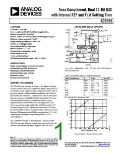
AD5399
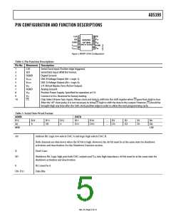
PIN CONFIGURATION AND FUNCTION DESCRIPTIONS
CLK
SDI
1
2
3
4
5
10 CS
V
V
9
8
7
6
TP
AD5399
DGND
TOP VIEW
DD
(Not to Scale)
V
AGND
OUTB
V
V
BZ
OUTA
Figure 3. MSOP-10 Pin Configuration
Table 4. Pin Function Descriptions
Pin No. Mnemonic Description
1
2
3
4
5
6
7
8
CLK
SDI
DGND
VOUTB
VOUTA
VBZ
AGND
VDD
VTP
Serial Clock Input. Positive edge triggered.
Serial Data Input. MSB first format.
Digital Ground.
DAC B Voltage Output (A0 = Logic 1).
DAC A Voltage Output (A0 = Logic 0).
2 V, Virtual Bipolar Zero (Active Output).
Analog Ground.
Positive Power Supply. Specified for operation at 5 V.
Connect to VDD. Reserved for factory testing.
9
10
CS
Chip Select (Frame Sync Input). Allows clock and data to shift into the shift register when CS goes from high to low.
After the 16th clock pulse, it is not necessary to bring CS high to shift the data to the output. However, CS should be
brought high any time after the 16th clock positive edge in order to allow the next programming cycle.
Table 5. Serial Data-Word Format
ADDR
DATA
B11
B15
A0
B14
X
B13
SD
B12
0
B10
D10
…
…
B3
B2
B1
B0
D11
D3
D2
D1
D0
LSB
MSB
Aꢀ
Address Bit. Logic low selects DAC A and logic high selects DAC B.
Both channels are shut down when the SD bit is high. However, the Aꢀ bit must be at the same state for shutdown
activation and deactivation. See the Shutdown Function section.
X
Don’t Care.
SD
Shutdown Bit. Logic high puts both DAC outputs and VBZ into high impedance. Aꢀ bit must be at the same state for
shutdown activation and deactivation.
ꢀ
B12 must be ꢀ.
Data Bits.
Dꢀ–D11
Rev. D | Page 5 of 12

 ADI [ ADI ]