Data Sheet
AD5290
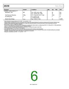
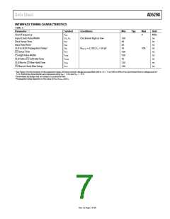
INTERFACE TIMING CHARACTERISTICS
Table 3.
Parameter
1, 2
Symbol
Conditions
Min
Typ
Max
Unit
MHz
ns
Clock Frequency
Input Clock Pulse Width
Data Setup Time
fCLK
tCH, tCL
tDS
4
Clock level high or low
120
30
ns
Data Hold Time
CLK to SDO Propagation Delay3
tDH
tPD
20
10
ns
ns
RPull-up = 2.2 kΩ, CL < 20 pF
100
CS Setup Time
tCSS
120
150
10
ns
CS High Pulse Width
CLK Fall to CS Fall Hold Time
CLK Rise to CS Rise Hold Time
CS Rise to Clock Rise Setup
tCSW
tCSH0
tCSH
tCS1
ns
ns
120
120
ns
ns
1 See Figure 3 for the location of the measured values. All input control voltages are specified with tR = tF = 1 ns (10% to 90% of VDD) and timed from a voltage level of
1.6 V. Switching characteristics are measured using VDD = +15 V and VSS = −15 V.
2 Guaranteed by design and not subject to production test.
3 Propagation delay depends on the value of VDD, RPull-up, and CL.
Rev. C | Page 7 of 20

 ADI [ ADI ]