AD5290
Data Sheet
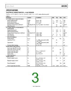
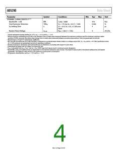
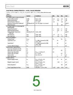
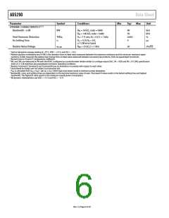
Parameter
DYNAMIC CHARACTERISTICS6, 8, 9
Symbol
Conditions
Min
Typ1
Max
Unit
Bandwidth −3 dB
BW
RAB = 50 kΩ, code = 0x80
RAB = 100 kΩ, code = 0x80
VA = 1 V rms, VB = 0 V, f = 1 kHz
VA = 10 V, VB = 0 V,
1 LSB error band
90
50
0.002
4
kHz
kHz
%
Total Harmonic Distortion
VW Settling Time
THDW
tS
µs
Resistor Noise Voltage
eN_WB
RWB = 25 kΩ, f = 1 kHz
20
nV√Hz
1 Typical represents average reading at +25°C, VDD = +15 V, and VSS = −15 V.
2 Resistor position nonlinearity error R-INL is the deviation from an ideal value measured between the maximum resistance and the minimum resistance wiper
positions. R-DNL measures the relative step change from an ideal value measured between successive tap positions. Parts are guaranteed monotonic.
3 All parts have a 35 ppm/°C temperature coefficient.
4 INL and DNL are measured at VW with the RDAC configured as a potentiometer divider similar to a voltage output DAC. VA = VDD and VB = 0 V. DNL specification
limits of 1 LSB maximum are guaranteed monotonic operating conditions.
5 Resistor Terminal A, Terminal B, and Terminal W have no limitations on polarity with respect to each other.
6 Guaranteed by design and not subject to production test.
7 PDISS is calculated from (IDD × VDD) + abs (ISS × VSS). CMOS logic level inputs result in minimum power dissipation.
8 Bandwidth, noise, and settling times are dependent on the terminal resistance value chosen. The lowest R value results in the fastest settling time and highest
bandwidth. The highest R value results in the minimum overall power consumption.
9 All dynamic characteristics use VDD = +15 V and VSS = −15 V.
Rev. C | Page 6 of 20

 ADI [ ADI ]