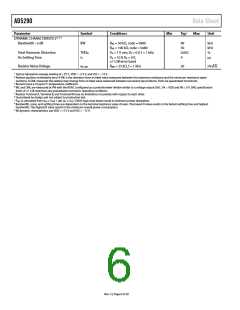
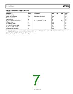
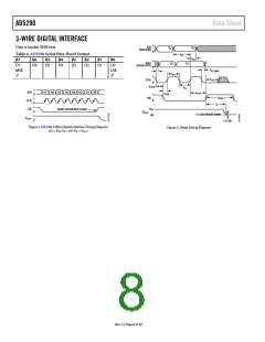
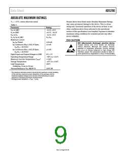
AD5290
Data Sheet
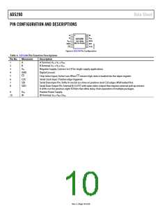
PIN CONFIGURATION AND DESCRIPTIONS
A
B
1
2
3
4
5
10
9
W
V
DD
AD5290
TOP VIEW
(Not to Scale)
V
8
SDO
SDI
SS
GND
CS
7
6
CLK
Figure 4. AD5290 Pin Configuration
Table 6. AD5290 Pin Function Descriptions
Pin No.
Mnemonic
Description
1
2
3
4
5
6
7
8
A
B
VSS
GND
CS
A Terminal. VSS ≤ VA ≤ VDD.
B Terminal. VSS ≤ VB ≤ VDD.
Negative Supply. Connect to 0 V for single-supply applications.
Digital Ground.
CS
Chip Select Input; Active Low. When returns high, data is loaded into the wiper register.
Serial Clock Input. Positive edge triggered.
Serial Data Input Pin. Shifts in one bit at a time on positive clock CLK edges. MSB loaded first.
Serial Data Output Pin. Internal N-Ch FET with open-drain output that requires external pull-up resistor.
It shifts out the previous eight SDI bits that allow daisy-chain operation of multiple packages.
CLK
SDI
SDO
9
10
VDD
W
Positive Power Supply.
W Terminal. VSS ≤ VW ≤ VDD.
Rev. C | Page 10 of 20

 ADI [ ADI ]