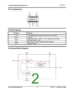
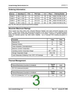
Acutechnology Semiconductor Inc.
AQ8211
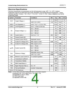
Electrical Specifications
Electrical characteristics are guaranteed over the full temperature range -40ºC <Tj< 125ºC. Ambient
temperature must be de-rated based upon power dissipation and package thermal characteristics. Unless
otherwise specified: VENABLE = VIN = (VOUT + 1.5V), IOUT = 10 mA, Tj = 25C. Values in bold are over the full
temperature range.
Symbol Parameter
Conditions
Min
Typ
Max Units
-1
VOUT
VOUT
0.035
0.2
+1
+1.5
0.2
%
%
VOUT
Output Voltage (1)
-1.5
-40°C ≤Tj ≤ 125°C
∆VEN = VOUT + (1.5V to 10V)
∆IOUT = (10mA to 250 mA)
IOUT = 100 mA
LNREG
LDREG
Line Regulation (1)
Load Regulation (1)
%
0.4
%
50
80
mV
mV
mV
mA
µA
µA
V
VD
Dropout Voltage (1, 2)
IOUT = 250 mA
150
300
800
100
65
200
350
IOUT = 500 mA
ISC
IGND
IGND
VIL
Current Limit (1)
VEN-VOUT = 2V
600
Ground Current ON
150
100
Ground Current ON (5)
Enable Pin Voltage (OFF)
Enable Pin Voltage (ON)
Adjustable version
With respect to GND
With respect to VOUT
IOUT = 10 mA
0.25
0.45
0.92
0.3
VIH
0.95
0.5
V
mA
mA
mA
V
IENON
Enable Current ON
IOUT = 250 mA
1.8
3.0
IOUT = 500 mA
3.8
5.0
Adjustable version only
-40°C ≤Tj ≤ 125°C
To maintain regulation
1.208 1.220 1.232
VADJ
Reference Voltage
1.202
1.238
2.0
V
IQMIN
TC
Minimum Load Current (5)
Temperature Coefficient
Temperature Stability
0.5
0.005
0.5
mA
%/°C
%/°C
TS
%
VN
RMS Output Noise (3)
0.003
VOUT
PSRR
TSD
Ripple Rejection Ratio (4)
Thermal Shutdown
Vin = 5V
60
72
150
25
dB
°C
°C
Junction Temperature
TSDHYST TSD Hysteresis
Notes: (1) Low duty cycle pulse testing with Kelvin connections required.
(2) Measure (VIN - VOUT) when ∆VOUT, OR ∆VREF = 1%
(3) Bandwidth of 10Hz to 10kHz
(4) 120Hz input ripple
(5) Adjustable version only
www.acutechnology.com
4
Rev. 2.1 January 22, 2006

 ACUTECH [ ACUTECHNOLOGY SEMICONDUCTOR ]