ACE24LC02/04/08/16
Two-wire Serial EEPROM
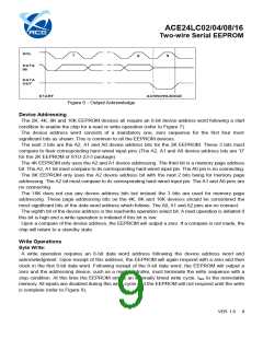
Figure 6.Output Acknowledge
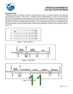
Device Addressing
The 2K, 4K, 8K and 16K EEPROM devices all require an 8-bit device address word following a start
condition to enable the chip for a read or write operation (refer to Figure 7).
The device address word consists of a mandatory one, zero sequence for the first four most
significant bits as shown. This is common to all the EEPROM devices.
The next 3 bits are the A2, A1 and A0 device address bits for the 2K EEPROM. These 3 bits must
compare to their corresponding hard-wired input pins (The A2, A1 and A0 device address bits are “0”
for the 2K EEPROM of STO-23-5 package)
The 4K EEPROM only uses the A2 and A1 device addressing. The third bit is a memory page address
bit. The A2, A1 bit must compare to its corresponding hard-wired input pin. The A0 pin is no connecting.
The 8K EEPROM only uses the A2 device address bit with the next 2 bits being for memory page
addressing. The A2 bit must compare to its corresponding hard-wired input pin. The A1 and A0 pins are
no connecting.
The 16K does not use any device address bits but instead the 3 bits are used for memory page
addressing. These page addressing bits on the 4K, 8K and 16K devices should be considered the
most significant bits of the data word address which follows. The A0, A1 and A2 pins are no connect.
The eighth bit of the device address is the read/write operation select bit. A read operation is initiated if
this bit is high and a write operation is initiated if this bit is low.
Upon a compare of the device address, the EEPROM will output a zero. If a compare is not made, the
chip will return to a standby state.
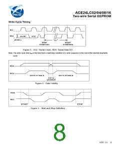
Write Operations
Byte Write:
A write operation requires an 8-bit data word address following the device address word and
acknowledgment. Upon receipt of this address, the EEPROM will again respond with a zero and then
clock in the first 8-bit data word. Following receipt of the 8-bit data word, the EEPROM will output a
zero and the addressing device, such as a microcontroller, must terminate the write sequence with a
stop condition. At this time the EEPROM enters an internally timed write cycle, tWR, to the nonvolatile
memory. All inputs are disabled during this write cycle and the EEPROM will not respond until the write
is complete (refer to Figure 8).
VER 1.6
9

 ACE [ ACE TECHNOLOGY CO., LTD. ]