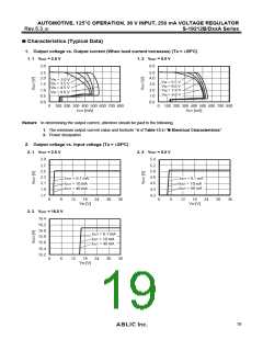
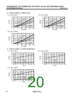
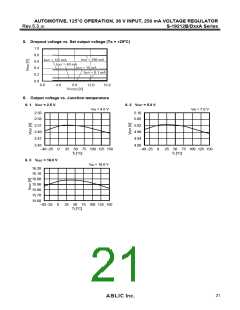
AUTOMOTIVE, 125°C OPERATION, 36 V INPUT, 250 mA VOLTAGE REGULATOR
S-19212B/DxxA Series
Rev.5.3_00
Precautions
• Generally, when a voltage regulator is used under the condition that the load current value is small (0.1 mA or less),
the output voltage may increase due to the leakage current of an output transistor.
• Generally, when a voltage regulator is used under the condition that the temperature is high, the output voltage may
increase due to the leakage current of an output transistor.
• Generally, when the ON / OFF pin is used under the condition of OFF, the output voltage may increase due to the
leakage current of an output transistor.
• Generally, when a voltage regulator is used under the condition that the impedance of the power supply is high, an
oscillation may occur. Perform thorough evaluation including the temperature characteristics with an actual
application to select CIN.
• Generally, in a voltage regulator, an oscillation may occur depending on the selection of the external parts. The
following use conditions are recommended in the S-19212B/DxxA Series, however, perform thorough evaluation
including the temperature characteristics with an actual application to select CIN and CL.
Input capacitor (CIN): A ceramic capacitor with capacitance of 1.0 μF or more is recommended.
Output capacitor (CL): A ceramic capacitor with capacitance of 1.0 μF to 100 μF is recommended.
• Generally, in a voltage regulator, the values of an overshoot and an undershoot in the output voltage vary
depending on the variation factors of input voltage start-up, input voltage fluctuation and load fluctuation etc., or the
capacitance of CIN or CL and the value of the equivalent series resistance (ESR), which may cause a problem to the
stable operation. Perform thorough evaluation including the temperature characteristics with an actual application to
select CIN and CL.
• Generally, in a voltage regulator, an overshoot may occur in the output voltage momentarily if the input voltage
steeply changes when the input voltage is started up or the input voltage fluctuates etc. Perform thorough evaluation
including the temperature characteristics with an actual application to confirm no problems happen.
• Generally, in a voltage regulator, if the VOUT pin is steeply shorted with GND, a negative voltage exceeding the
absolute maximum ratings may occur in the VOUT pin due to resonance phenomenon of the inductance and the
capacitance including CL on the application. The resonance phenomenon is expected to be weakened by inserting a
series resistor into the resonance path, and the negative voltage is expected to be limited by inserting a protection
diode between the VOUT pin and the VSS pin.
• If the input voltage is started up steeply under the condition that the capacitance of CL is large, the thermal
shutdown circuit may be in the detection status by self-heating due to the charge current to CL.
• Make sure of the conditions for the input voltage, output voltage and the load current so that the internal loss does
not exceed the power dissipation.
• Do not apply an electrostatic discharge to this IC that exceeds the performance ratings of the built-in electrostatic
protection circuit.
• When considering the output current value that the IC is able to output, make sure of the output current value
specified in Table 13 in " Electrical Characteristics" and footnote *4 of the table.
• Wiring patterns on the application related to the VIN pin, the VOUT pin and the VSS pin should be designed so that
the impedance is low. When mounting CIN between the VIN pin and the VSS pin and CL between the VOUT pin and
the VSS pin, connect the capacitors as close as possible to the respective destination pins of the IC.
• In the package equipped with heat sink of backside, mount the heat sink firmly. Since the heat radiation differs
according to the condition of the application, perform thorough evaluation with an actual application to confirm no
problems happen.
• ABLIC Inc. claims no responsibility for any disputes arising out of or in connection with any infringement by products
including this IC of patents owned by a third party.
18

 ABLIC [ ABLIC ]