AUTOMOTIVE, 125°C OPERATION, 36 V INPUT, 250 mA VOLTAGE REGULATOR
S-19212B/DxxA Series
Rev.5.3_00
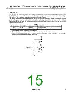
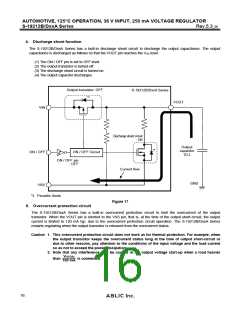
4. Discharge shunt function
The S-19212B/DxxA Series has a built-in discharge shunt circuit to discharge the output capacitance. The output
capacitance is discharged as follows so that the VOUT pin reaches the VSS level.
(1) The ON / OFF pin is set to OFF level.
(2) The output transistor is turned off.
(3) The discharge shunt circuit is turned on.
(4) The output capacitor discharges.
Output transistor: OFF
S-19212B/DxxA Series
*1
VOUT
VIN
Discharge shunt circuit
: ON
Output
capacitor
(CL)
*1
ON / OFF
ON / OFF Circuit
ON / OFF pin
: OFF
Current flow
GND
VSS
*1. Parasitic diode
Figure 17
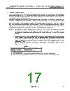
5. Overcurrent protection circuit
The S-19212B/DxxA Series has a built-in overcurrent protection circuit to limit the overcurrent of the output
transistor. When the VOUT pin is shorted to the VSS pin, that is, at the time of the output short-circuit, the output
current is limited to 120 mA typ. due to the overcurrent protection circuit operation. The S-19212B/DxxA Series
restarts regulating when the output transistor is released from the overcurrent status.
Caution 1. This overcurrent protection circuit does not work as for thermal protection. For example, when
the output transistor keeps the overcurrent status long at the time of output short-circuit or
due to other reasons, pay attention to the conditions of the input voltage and the load current
so as not to exceed the power dissipation.
2. Note that any interference may be caused in the output voltage start-up when a load heavier
VOUT(S)
than
is connected.
100 mA
16

 ABLIC [ ABLIC ]