AUTOMOTIVE, 125°C OPERATION, 36 V INPUT, 250 mA VOLTAGE REGULATOR
S-19212B/DxxA Series
Rev.5.3_00
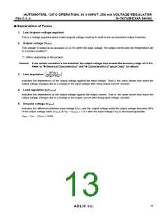
Operation
1. Basic operation
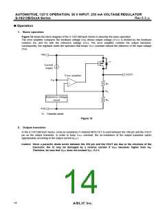
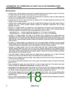
Figure 15 shows the block diagram of the S-19212B/DxxA Series to describe the basic operation.
The error amplifier compares the feedback voltage (Vfb) whose output voltage (VOUT) is divided by the feedback
resistors (Rs and Rf) with the reference voltage (Vref). The error amplifier controls the output transistor,
consequently, the regulator starts the operation that keeps VOUT constant without the influence of the input voltage
(VIN).
VIN
*1
Current
supply
VOUT
Error amplifier
−
+
Vref
Rf
Vfb
Reference voltage
circuit
Rs
VSS
*1. Parasitic diode
Figure 15
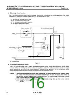
2. Output transistor
In the S-19212B/DxxA Series, a low on-resistance P-channel MOS FET is used between the VIN pin and the VOUT
pin as the output transistor. In order to keep VOUT constant, the on-resistance of the output transistor varies
appropriately according to the output current (IOUT).
Caution Since a parasitic diode exists between the VIN pin and the VOUT pin due to the structure of the
transistor, the IC may be damaged by a reverse current if VOUT becomes higher than VIN.
Therefore, be sure that VOUT does not exceed VIN + 0.3 V.
14

 ABLIC [ ABLIC ]