AAT3681
USB Port or AC Adapter
Lithium-Ion/Polymer Battery Charger
Where:
Capacitor Selection
Input Capacitor
PD = Total Power Dissipation by the Device
VIN = Input Voltage
In general, it is good design practice to place a
decoupling capacitor between the ADP pin and
GND. An input capacitor in the range of 1µF to
22µF is recommended. If the source supply is
unregulated, it may be necessary to increase the
capacitance to keep the input voltage above the
under-voltage lockout threshold during device
enable and when battery charging is initiated. If the
AAT3681 adapter input is to be used in a system
with an external power supply source, such as a
typical AC-to-DC wall adapter, then a CIN capacitor
in the range of 10µF should be used. A larger input
capacitor in this application will minimize switching
or power transient effects when the power supply is
"hot plugged" in.
VBAT = Battery Voltage as Seen at the BAT Pin
ICH = Constant Charge Current Programmed for
the Application
IOP = Quiescent Current Consumed by the
Charger IC for Normal Operation [0.5mA]
By substitution, we can derive the maximum
charge current before reaching the thermal limit
condition (thermal cycling). The maximum charge
current is the key factor when designing battery
charger applications.
(PD(MAX)
-
VIN
VIN - VBAT
· IOP)
Output Capacitor
ICH(MAX)
=
The AAT3681 only requires a 1µF ceramic capaci-
tor on the BAT pin to maintain circuit stability. This
value should be increased to 10µF or more if the
battery connection is made any distance from the
charger output. If the AAT3681 is to be used in
applications where the battery can be removed
from the charger, such as with desktop charging
cradles, an output capacitor greater than 10µF may
be required to prevent the device from cycling on
and off when no battery is present.
(TJ(MAX)
θJA
VIN - VBAT
- TA)
-
VIN · IOP
ICH(MAX)
=
In general, the worst condition is the greatest volt-
age drop across the charger IC, when battery volt-
age is charged up to the preconditioning voltage
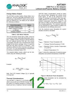
threshold. Figure 4 shows the maximum charge
current in different ambient temperatures.
Printed Circuit Board Layout
Considerations
300
TA = 25°C
For the best results, it is recommended to physically
place the battery pack as close as possible to the
AAT3681 BAT pin. To minimize voltage drops on the
PCB, keep the high current carrying traces ade-
quately wide. Refer to the AAT3681 evaluation board
for a good layout example (see Figures 5 and 6).
250
TA = 45°C
200
150
TA = 60°C
100
TA = 85°C
50
0
4.25 4.5 4.75
5
5.25 5.5 5.75
6
6.25 6.5 6.75
VIN (V)
Figure 4: Maximum Charging Current Before
Thermal Cycling Becomes Active.
3681.2007.01.1.2
13

 AAT [ ADVANCED ANALOG TECHNOLOGY, INC. ]