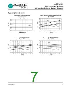
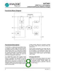
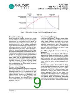
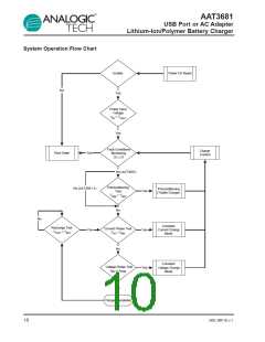
AAT3681
USB Port or AC Adapter
Lithium-Ion/Polymer Battery Charger
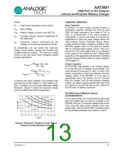
160°C/W. Many considerations should be taken
into account when designing the printed circuit
board layout, as well as the placement of the
charger IC package in proximity to other heat gen-
erating devices in a given application design. The
ambient temperature around the charger IC will
also have an effect on the thermal limits of a bat-
tery charging application. The maximum limits that
can be expected for a given ambient condition can
be estimated by the following discussion.
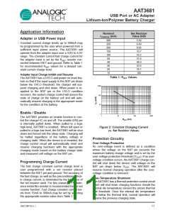
Charge Status Output
The AAT3681 provides battery charge status via a
status pin. This pin is internally connected to an N-
channel open drain MOSFET, which can be used to
drive an external LED. The status pin can indicate
the following conditions:
Event Description
Status
No battery charging activity
Battery charging via adapter
or USB port
OFF
First, the maximum power dissipation for a given
situation should be calculated:
ON
Charging completed
OFF
Table 2: LED Status Indicator.
(TJ(MAX) - TA)
θJA
PD(MAX)
=
The LED should be biased with as little current as
necessary to create reasonable illumination; there-
fore, a ballast resistor should be placed between
the LED cathode and the STAT pin. LED current
consumption will add to the overall thermal power
budget for the device package, hence it is good to
keep the LED drive current to a minimum. 2mA
should be sufficient to drive most low-cost green or
red LEDs. It is not recommended to exceed 8mA
for driving an individual status LED.
Where:
PD(MAX) = Maximum Power Dissipation (W)
θJA = Package Thermal Resistance (°C/W)
TJ(MAX) = Maximum Device Junction Temperature
(°C) [135°C]
TA
= Ambient Temperature (°C)
The required ballast resistor values can be esti-
mated using the following formulas:
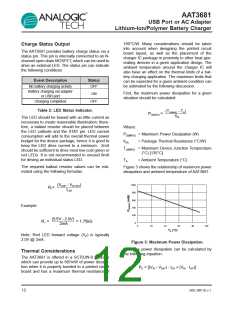
Figure 3 shows the relationship of maximum power
dissipation and ambient temperature of AAT3681.
1000
800
600
400
200
0
(VADP
-
ILED
VF(LED)
)
R1=
Example:
(5.5V - 2.0V)
2mA
R1 =
= 1.75kΩ
0
20
40
60
80
100
TA (°C)
Note: Red LED forward voltage (VF) is typically
2.0V @ 2mA.
Figure 3: Maximum Power Dissipation.
Next, the power dissipation can be calculated by
the following equation:
Thermal Considerations
The AAT3681 is offered in a SC70JW-8 package
which can provide up to 687mW of power dissipa-
tion when it is properly bonded to a printed circuit
board and has a maximum thermal resistance of
PD = [(VIN - VBAT
)
·
ICH + (VIN
·
IOP)]
12
3681.2007.01.1.2

 AAT [ ADVANCED ANALOG TECHNOLOGY, INC. ]