BRIGHT
Microelectronics
Inc.
BM29F400T/BM29F400B
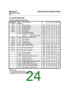
AC CHARACTERISTICS
Programming/Erase Operations
PARAMETER SYM.
DESCRIPTION
-90
-120 -150 UNIT
JEDEC
Standard
(1)
Write Cycle Time
t
t
Min.
Min.
Min.
Min.
Min.
Min.
Min.
Min.
90
0
120
0
150
0
nS
nS
nS
nS
nS
nS
nS
nS
AVAV
WC
t
t
Address Setup Time
Address Hold Time
Data Setup Time
AVWL
AS
AH
DS
DH
t
t
t
45
45
0
50
50
0
50
50
0
WLAX
t
DVWH
t
t
Data Hold Time
WHDX
t
Output Enable Setup Time
0
0
0
OES
OEH
(1)
Read
t
Output Enable
Hold Time
0
0
0
10
10
10
(1)
Polling
Toggle &
Data
t
t
Read Recover Time Before Write
Min.
Min.
0
0
0
0
0
0
nS
nS
GHWL
GHWL
t
t
ELWL
CS
Setup Time
Hold Time
CE
CE
t
t
Min.
0
0
0
nS
WHEH
CH
t
t
t
Write Pulse Width
Min.
Min.
45
20
50
20
50
20
nS
nS
WLWH
WHWL
WP
t
Write Pulse Width High
Byte Programming Operation
WPH
t
t
t
t
Typ.
Max.
16
400
16
400
16
400
S
m
WHWH1
WHWH2
WHWH3
WHWH1
S
m
(2)
t
Sector Erase Operation
Typ.
Max.
0.26
12
0.26
12
0.26
12
sec
WHWH2
(2)
Chip Erase Operation
t
Typ.
Max.
2.0
90
2.0
90
2.0
90
sec
WHWH3
(1)
Vcc Setup Time
t
Min.
Min.
Min.
50
500
4
50
500
4
50
500
4
mS
nS
VCS
Rise Time to VID(1,3)
t
VIDR
t
mS
OESP
(1, 3, 4)
Active
Setup Time to
OE
WE
t
Min.
Min.
500
4
500
4
500
4
nS
RP
Pulse Width
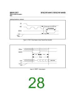
RESET
t
S
m
RSP
( 3)
Setup Time
RESET
(1)
Programming/Erase Valid to RY/BY Delay
t
Min.
Min.
Min.
Min.
Min.
40
4
50
4
60
4
nS
mS
mS
mS
nS
BUSY
(1, 4)
Voltage Transition Time
t
VLHT
(4)
(4)
t
t
Sector Protect Write Pulse Width
Sector Unprotect Write Pulse Width
(1, 4)
100
350
4
100
350
4
100
350
4
WPP1
WPP2
t
CSP
Setup Time to
Active
WE
CE
Notes:
1. Not 100% tested.
2. Does not include pre-programming time.
3. This timing is for Temporary Sector Unprotect operation.
These timings are for Sector Protect and/or Sector Unprotect operations.
- 24 -

 WINBOND [ WINBOND ]