BRIGHT
Microelectronics
Inc.
BM29F400T/BM29F400B
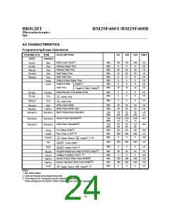
AC CHARACTERISTICS
Read-only Operations
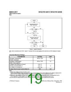
DESCRIPTION
-90
-120 -150 UNIT
PARAMETER
SYM.
TEST SETUP
JEDEC
Standard
(2)
Read Cycle Time
Min.
90
90
120
120
150
150
nS
nS
t
t
t
t
AVAV
RC
Address to Output Delay
Max.
CE
OE = V
IL
IL
AVQV
ACC
= V
Chip Enable to Output Delay
Output Enable to Output Delay
Max.
90
120
150
nS
t
t
IL
ELQV
CE
OE = V
Max.
Max.
35
20
50
30
55
35
nS
nS
t
t
t
t
GLQV
OE
HZ
Chip Enable to Output High
Z(3,4)
EHQZ
Output Enable to Output High
Z(2,3)
20
0
30
0
35
0
nS
nS
t
t
t
GHQZ
AXQX
DF
Output Hold Time from
Addresses, CE or OE ,
Whichever Occurs First
Min.
t
OH
t
Max.
Max.
20
5
20
5
20
5
mS
nS
READY
RESET Pin Low to Read
Mode
(4)
t
t
ELFL
ELFH
CE
BYTE
Switching Low or
to
High
Notes:
1. Test Conditions: Output Load: 1 TTL gate and 100 pF
Input rise and fall times: 20 nS; Input pulse levels: 0V to 3 V
2. Timing measurement reference level
Input/Output: 1.5V
3. Output driver disable time.
4. Not 100% tested.
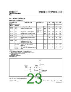
5.0 V
2.7 KOhm
IN3064 or
Equivalent
DEVICE
UNDER
TEST
CL
6.2 KOhm
Diodes = IN3064
or Equivalent
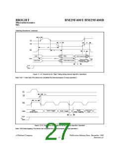
Figure 7. Test Condition
Note: CL = 100 pF including jig capacitance.
A Winbond Company
Publication Release Date: December 1999
Revision A2
- 23 -

 WINBOND [ WINBOND ]