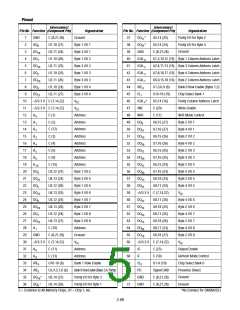
Pinout
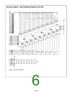
Interconnect
Pin No. Function (Component Pin)
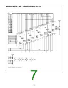
Interconnect
Organization
Pin No. Function (Component Pin)
Organization
Parity I/O for Byte 2
Parity I/O for Byte 4
Ground
1
2
GND
DQ0
C (8,21,28)
U1,10 (27)
U2,11 (24)
U1,10 (26)
U2,11 (25)
U1,10 (25)
U2,11 (26)
U1,10 (24)
U2,11 (27)
Ground
37
38
39
40
41
42
43
44
45
46
47
48
49
50
51
52
53
54
55
56
57
58
59
60
61
62
63
64
65
66
67
68
69
70
71
72
DQ17*
DQ35*
GND
/CAL0
/CAL2
/CAL3
/CAL1
/RE0
U5,14 (25)
U5,14 (24)
C (8,21,28)
Byte 1 I/O 1
Byte 3 I/O 1
Byte 1 I/O 2
Byte 3 I/O 2
Byte 1 I/O 3
Byte 3 I/O 3
Byte 1 I/O 4
Byte 3 I/O 4
3
DQ18
DQ1
4
U1,3,10,12 (16) Byte 1 Column Address Latch
U2,4,11,13 (16) Byte 3 Column Address Latch
U7,8,16,17 (16) Byte 4 Column Address Latch
U6,9,15,18 (16) Byte 2 Column Address Latch
5
DQ19
DQ2
6
7
DQ20
DQ3
8
U1,3,6,9 (6)
U10-18 (19)
U5,14 (16)
C (20)
Bank 0 Row Enable (Bytes 1,2)
Chip Select Bank 1
Parity Column Address Latch
Write Enable
9
DQ21
/S1
10
11
12
13
14
15
16
17
18
19
20
21
22
23
24
25
26
27
28
29
30
31
32
33
34
35
36
+5/3.3 V C (7,14,22)
+5/3.3 V C (7,14,22)
V
/CALP*
/WE
CC
V
CC
A0
C (1)
Address
W/R
C (17)
W/R Mode Control
Byte 2 I/O 1
A1
C (2)
Address
DQ9
U6,15 (27)
U7,16 (27)
U6,15 (26)
U7,16 (26)
U6,15 (25)
U7,16 (25)
U6,15 (24)
U7,16 (24)
U9,18 (24)
U8,17 (24)
A2
C (12)
Address
DQ27
DQ10
DQ28
DQ11
DQ29
DQ12
DQ30
DQ13
DQ31
Byte 4 I/O 1
A3
C (3)
Address
Byte 2 I/O 2
A4
C (4)
Address
Byte 4 I/O 2
A5
C (5)
Address
Byte 2 I/O 3
A6
C (9)
Address
Byte 4 I/O 3
A10
DQ4
DQ22
DQ5
DQ23
DQ6
DQ24
DQ7
DQ25
A7
C (15)
Address
Byte 2 I/O 4
U3,12 (27)
U4,13 (24)
U3,12 (26)
U4,13 (25)
U3,12 (25)
U4,13 (26)
U3,12 (24)
U4,13 (27)
C (10)
Byte 1 I/O 5
Byte 3 I/O 5
Byte 1 I/O 6
Byte 3 I/O 6
Byte 1 I/O 7
Byte 3 I/O 7
Byte 1 I/O 8
Byte 3 I/O 8
Address
Byte 4 I/O 4
Byte 2 I/O 5
Byte 4 I/O 5
+5/3.3 V C (7,14,22)
V
CC
DQ32
DQ14
DQ33
DQ15
DQ34
DQ16
U8,17 (26)
U9,18 (25)
U8,17 (25)
U9,18 (26)
U8,17 (24)
U9,18 (27)
Byte 4 I/O 6
Byte 2 I/O 6
Byte 4 I/O 7
Byte 2 I/O 7
Byte 4 I/O 8
Byte 2 I/O 8
GND
C (8,21,28)
Ground
+5/3.3 V C (7,14,22)
V
+5/3.3 V C (7,14,22)
V
CC
CC
A8
A9
C (11)
Address
/G
C (23)
Output Enable
C (13)
Address
/F
C (18)
Refresh Mode Control
Chip Select Bank 0
Presence Detect
Ground
/RE
U10-18 (6)
U2,4,5,7,8 (6)
U5,14 (27)
U5,14 (26)
Bank 1 Row Enable
Bank 0 Row Enable (Bytes 3,4, Parity)
Parity I/O for Byte 3
Parity I/O for Byte 1
/S0
PD
GND
GND
U1-9 (19)
Signal GND
C (8,21,28)
C (8,21,28)
3
/RE
2
DQ26*
DQ8*
Ground
C = Common to All Memory Chips, U1 = Chip 1, etc.
*No Connect for DM2M32SJ
2-99

 RAMTRON [ RAMTRON INTERNATIONAL CORPORATION ]