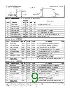
coherency. Random or page mode writes can be posted 5ns after
column address and data are available. The EDRAM allows 12ns
page mode cycle time for both write hits and write misses. Memory
writes do not affect the contents of the cache row register except
during a cache hit.
By integrating the SRAM cache as row registers in the DRAM
array and keeping the on-chip control simple, the EDRAM is able
to provide superior performance over standard slow DRAMs. By
eliminating the need for SRAMs and cache controllers, system cost,
board space, and power can all be reduced.
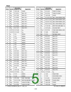
EDRAM Basic Operating Modes
The EDRAM operating modes are specified in the table.
Hit and Miss Terminology
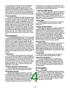
In this datasheet, “hit” and “miss” always refer to a hit or miss
to any of the four pages of data contained in the SRAM cache row
registers. There are four cache row registers, one for each of the
four banks of DRAM. These registers are specified by the bank
select row address bits A and A . The contents of these cache row
2
9
registers is always equal to the last row that was read from each of
the four internal DRAM banks (as modified by any write hit data).
Functional Description
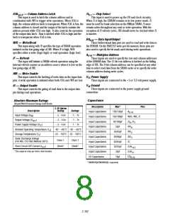
Bank Selection
The EDRAM is designed to provide optimum memory
performance with high speed microprocessors. As a result, it is
possible to perform simultaneous operations to the DRAM and
SRAM cache sections of the EDRAM. This feature allows the EDRAM
to hide precharge and refresh operation during SRAM cache reads
and maximize SRAM cache hit rate by maintaining valid cache
contents during write operations even if data is written to another
memory page. These new functions, in conjunction with the faster
basic DRAM and cache speeds of the EDRAM, minimize processor
wait states.
The 8MByte EDRAM SIMM has two separate 4MByte banks on
one module. The two banks share common data, multiplexed
address, and control signals with the exception of /RE and /S. Bank
selection is performed by using both /RE and /S to select a bank.
The use of /S to select a bank is required on the 8MByte SIMM
because /G is common between the two banks. If /S is grounded
(i.e., not used to control bank selection), an output buffer conflict
between the two banks will occur when /G is enabled. It is also
necessary to clock the /RE signal for each bank separately since
clocking /RE with /S disabled is not allowed (see “Unallowed
Mode” description).
Four Bank Cache Architecture (One of Two Banks)
Bank 3
Bank 2
Bank 1
Bank 0
Last
Row
Read
Address
Latch
+ 9-Bit
Compare
RA
0-10
CA
0-8
D0-35
1MB Array
1MB Array
1MB Array
1MB Array
A
Data-In
Latch
0-10
512 x 36
Cache
512 x 36
Cache
512 x 36
Cache
512 x 36
Cache
CA
0-8
Bank 0
Bank 1
Bank 2
Bank 3
(0,0)
(0,1)
(1,0)
(1,1)
1 of 4 Selector
RA , RA
2
9
Data-Out
Latch
CAL
G
S
Q 0-35
2-96

 RAMTRON [ RAMTRON INTERNATIONAL CORPORATION ]