are brought high and tRE is satisfied), /RE can be brought high to
precharge the memory. It is possible to perform cache reads
concurrently with the precharge. During write sequences, a write
operation is not performed unless both /CAL and /WE are low. As a
result, /CAL can be used as a byte write select in multi-chip systems. If
/CAL is not clocked on a write sequence, the memory will perform a
/RE only refresh to the selected row and data will remain unmodified.
refresh period. A does not need to be cycled. Read refresh cycles
are not allowed because a DRAM refresh cycle does not occur when a
read refresh address matches the LRR address latch.
10
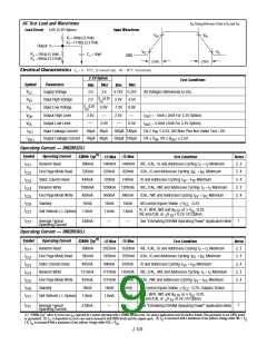
+3.3 Volt Power Supply Operation
If the +3.3 volt power supply option is specified, the EDRAM will
operate from a +3.3 volt +0.3 volt power supply and all inputs and
outputs will have LVTTL/LVCMOS compatible signal levels. The +3.3
volt EDRAM will not accept input levels which exceed the power
supply voltage. If mixed I/O levels are expected in your system, please
specify the +5 volt version of the EDRAM.
/RE Inactive Operation
It is possible to read data from the SRAM cache without clocking
/RE. This option is desirable when the external control logic is capable
of fast hit/miss comparison. In this case, the controller can avoid the
time required to perform row/column multiplexing on hit cycles. This
capability also allows the EDRAM to perform cache read operations
during precharge and refresh cycles to minimize wait states. It is only
necessary to select /S for the selected bank (/S or /S ) and /G and
Low Power Mode
The EDRAM enters its low power mode when /S is high. In this
mode, the internal DRAM circuitry is powered down to reduce
standby current.
0
1
Low Power, Self-Refresh Option
provide the appropriate column address to read data. The row address
of the SRAM cache accessed without clocking /RE will be specified by
the LRR address latch loaded during the last /RE active read cycle. To
perform a cache read, /CAL is clocked to latch the column address.
The cache data is valid at time tCLV after the column address is setup to
/CAL.
When the low power, self refresh mode option is specified when
ordering the EDRAM, the EDRAM enters this mode when /RE is
clocked while /S, W/R, /F, and /WE are high; and /CAL is low. In this
mode, the power is turned off to all I/O pins except /RE to minimize
chip power, and an on-board refresh clock is enabled to perform self-
refresh cycles using the on-board refresh counter. The EDRAM
remains in this low power mode until /RE is brought high again to
terminate the mode. The EDRAM /RE input must remain high for tRP2
following exit from self-refresh mode to allow any on-going internal
Write-Per-Bit Operation
The DM2M36SJ EDRAM SIMM provides a write-per-bit capability
to selectively modify individual parity bits (DQ8,17,26,35) for byte write
operations. The parity devices (DM2252) are selected via /CAL . Data refresh to terminate prior to the next memory operation.
bits do not require or support write-per-bit capability. Byte writPe
Initialization Cycles
A minimum of eight /RE active initialization cycle (read, write or
refresh) are required before normal operations is guaranteed.
selection to non-parity bits is accomplished via /CAL . The bits to be
0-3
written are determined by a bit mask data word which is placed on
the parity I/O data pins prior to clocking /RE. The logic one bits in the
Following these start-up cycles, two read cycles to different row
mask data select the bits to be written. As soon as the mask is latched
addresses must be performed for each of the four internal banks of
by /RE, the mask data is removed and write data can be placed on the
DRAM to initialize the internal cache logic. Row address bits A and
A define the four internal DRAM banks. /RE must be high for 2300ns
databus. The mask is only specified on the /RE transition. During page
9
mode burst write operations, the same mask is used for all write
prior to initialization.
operations.
Unallowed Mode
Read, write, or /RE only operations must not be initiated to
unselected memory banks by clocking /RE when /S is high.
Internal Refresh
If /F is active (low) on the assertion of /RE, an internal refresh
cycle is executed. This cycle refreshes the row address supplied by an
internal refresh counter. This counter is incremented at the end of the
cycle in preparation for the next /F refresh cycle. At least 1,024 /F
cycles must be executed every 64ms. /F refresh cycles can be hidden
because cache memory can be read under column address control
throughout the entire /F cycle. /F cycles are the only active cycles
during which /S can be disabled.
Reduced Pin Count Operation
It is possible to simplify the interface to the 8Mbyte SIMM to
reduce the number of control lines. /RE0 and /RE2 could be tied
together externally to provide a single row enable for bank 0. W/R
and /G can be tied together if reads are not performed during write
hit cycles. This external wiring simplifies the interface without any
performance impact.
/CAL Before /RE Refresh (“/CAS Before /RAS”)
/CAL before /RE refresh, a special case of internal refresh, is
discussed in the “Reduced Pin Count Operation” section below.
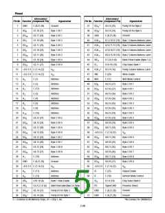
Pin Descriptions
/RE0,2,3 — Row Enable
This input is used to initiate DRAM read and write operations
and latch a row address as well as the states of W/R and /F. It is not
necessary to clock /RE to read data from the EDRAM SRAM row
registers. On read operations, /RE can be brought high as soon as
data is loaded into cache to allow early precharge. /RE to bank 0
and bank 1 must be clocked separately and only clocked during
DRAM operations to the selected bank.
/RE Only Refresh Operation
Although /F refresh using the internal refresh counter is the
recommended method of EDRAM refresh, it is possible to perform an
/RE only refresh using an externally supplied row address. /RE refresh
is performed by executing a write cycle (W/R and /F are high) where
/CAL is not clocked. This is necessary so that the current cache
contents and LRR are not modified by the refresh operation. All
combinations of addresses A must be sequenced every 64ms
0-9
2-98

 RAMTRON [ RAMTRON INTERNATIONAL CORPORATION ]