OX9162
OXFORD SEMICONDUCTOR LTD.
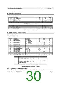
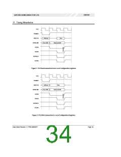
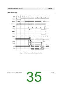
10 AC ELECTRICAL CHARACTERISTICS
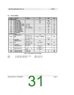
10.1 PCI Bus
The timings for PCI pins comply with PCI Specification for the 5.0 Volt signalling environment.
10.2 Local Bus
By default, the Local bus control signals change state in the cycle immediately following the reference cycle, with offsets to
provide setup and hold times for common peripherals in Intel mode. The tables below show these default values; however each
of these can be increased or decreased by an number of PCI clock cycles by adjusting the parameters in registers LT1 and LT2.
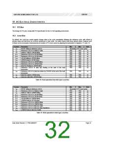
Symbol Parameter
Min
Max
Units
tref
tza
tard
tzrcs1
tzrcs2
tcsrd
trdcs
tzrd1
tzrd2
tdrd
IRDY# falling to reference LBCLK
Reference LBCLK to Address Valid
Address Valid to LBRD# falling
Reference LBCLK to LBCS# falling
Reference LBCLK to LBCS# rising
LBCS# falling to LBRD# falling
Nominally 2 PCI clock cycles
TBD
TBD
TBD
TBD
TBD
TBD
TBD
TBD
TBD
TBD
TBD
TBD
TBD
TBD
TBD
TBD
TBD
TBD
TBD
TBD
ns
ns
ns
ns
ns
ns
ns
ns
ns
ns
LBRD# rising to LBCS# rising
Reference LBCLK to LBRD# falling
Reference LBCLK to LBRD# rising
Data bus floating to LBRD# falling
Reference LBCLK to data bus floating at the start of the read
transaction
tzd1
tzd2
Reference LBCLK to data bus driven by OX9162 at the end of the read
transaction
TBD
TBD
ns
tsd
thd
Data bus valid to LBRD# rising
Data bus valid after LBRD# rising
TBD
TBD
TBD
TBD
ns
ns
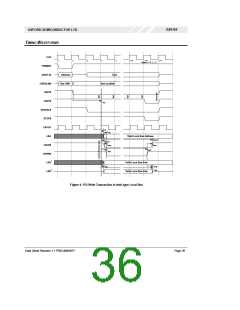
Table 18: Read operation from Intel-type Local Bus
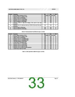
Symbol Parameter
Min
Max
Units
tref
tza
tawr
tzwcs1
tzwcs2
tcswr
twrcs
tzwr1
tzwr2
tzdv
IRDY# falling to reference LBCLK
Reference LBCLK to Address Valid
Address Valid to LBWR# falling
Reference LBCLK to LBCS# falling
Reference LBCLK to LBCS# rising
LBCS# falling to LBWR# falling
Nominally 2 PCI clock cycles
TBD
TBD
TBD
TBD
TBD
TBD
TBD
TBD
TBD
TBD
TBD
TBD
TBD
TBD
TBD
TBD
TBD
TBD
TBD
TBD
TBD
TBD
ns
ns
ns
ns
ns
ns
ns
ns
ns
ns
ns
LBWR# rising to LBCS# rising
Reference LBCLK to LBWR# falling
Reference LBCLK to LBWR# rising
Reference LBCLK to data bus valid
Reference LBCLK to data bus high-impedance
LBWR# rising to data bus invalid
tzdf
twrdi
Table 19: Write operation to Intel-type Local Bus
Data Sheet Revision 1.1 PRELIMINARY
Page 32

 OXFORD [ OXFORD SEMICONDUCTOR ]