OX9162
OXFORD SEMICONDUCTOR LTD.
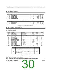
OPERATING CONDITIONS
8
Symbol
VDD
VIN
IIN
TSTG
Parameter
Min
-0.3
-0.3
Max
7.0
VDD + 0.3
+/- 10
125
Units
V
V
mA
°C
DC supply voltage
DC input voltage
DC input current
Storage temperature
-40
Table 14: Absolute maximum ratings
Symbol
VDD
TC
Parameter
DC supply voltage
Temperature
Min
4.5
0
Max
5.5
70
Units
V
°C
Table 15: Recommended operating conditions
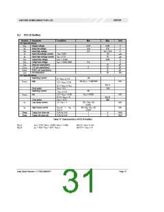
9
DC ELECTRICAL CHARACTERISTICS
9.1 Non-PCI I/O Buffers
Symbol Parameter
Condition
Commercial
TTL Interface 1
TTL Schmitt trig
TTL Interface 1
TTL Schmitt trig
Min
4.75
2.0
Max
5.25
Units
V
V
VDD
VIH
Supply voltage
Input high voltage
2.0
VIL
Input low voltage
0.8
0.8
5.0
10.0
10
V
CIL
COL
IIH
Cap of input buffers
pF
pF
mA
mA
V
V
V
V
mA
Cap of output buffers
Input high leakage current
Input low leakage current
Output high voltage
Output high voltage
Output low voltage
Vin = VDD
Vin = VSS
IOH = 1 mA
IOH = 4 mA 2
IOL = 1 mA
IOL = 4 mA 2
-10
-10
IIL
10
VDD – 0.05
VOH
VOH
VOL
VOL
IOZ
2.4
0.05
0.4
10
Output low voltage
3-state output leakage current
-10
Symbol Parameter
Typical
Max
Units
Operating supply current in
normal mode
TBD
TBD
ICC
mA
Operating supply current in
Power-down mode
TBD
Table 16: Characteristics of non-PCI I/O buffers
Note 1:
Note 2:
All input buffers are TTL with the exception of PCI buffers
and I are 12 mA for PD/LBDB[7:0] and other Parallel Port Outputs. They are 4 mA for all other non-PCI outputs
I
OH
OL
Data Sheet Revision 1.1 PRELIMINARY
Page 30

 OXFORD [ OXFORD SEMICONDUCTOR ]