FEDL87V2107-01
OKI Semiconductor
ML87V2107
2.4 Output System Settings
2.4.1 Output Data Setting
SUB_ADDRESS=60h(W/R): Output data setting
DATA_BIT
BIT7
BIT6
BIT5
BIT4
BIT3
0
BIT2
BIT1
BIT0
REFSL
(Reserved)
Register name CKEN
CKSL
CKINV
R656O
DOSEL
1
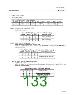
DOSEL Initial value: 0; Setting range: 0 to 1
Sets the output format.
Table R2-4-1 (1) Output Data Format Mode Setting
IRMON
MODE4
DOSEL
Output data format
0
1
0
1
0
X
1
X
0
X
1
16-bit 4:2:2 YCbCr
8-bit 4:2:2 YCbCr
X
R656O Initial value: 0; Setting range: 0 to 1
Sets an addition of an output timing reference code.
In memory output mode only, timing reference codes (SAV, EAV) complying with ITU-RBT.656 are
added to output data.
Table R2-4-1(2) Timing Reference Code Addition Setting
IRMON
MODE5
R656O
Timing reference code
0
1
0
1
0
X
1
X
0
X
1
None
Conforming to ITU-RBT. 656
X
REFSL Initial value: 00; Setting range: 00 to 11
Sets HREF pin output.
Selects and outputs any one of the horizontal reference signal, chrominance select signal, effective area
signal, and field pulse signal.
Table R2-4-1 (3) HREF Pin Output Selection
REFSL
HREF pin output
[0]
0
[1]
0
Horizontal reference signal
Chrominance select signal
Effective area signal
0
1
1
0
1
1
Field pulse signal
133/152

 OKI [ OKI ELECTRONIC COMPONETS ]