FEDL674000-02
OKI Semiconductor
ML674000
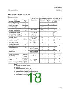
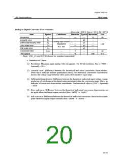
ELECTRICAL CHARACTERISTICS
DC Characteristics
(VDD_CORE = 2.25 to 2.75V, VDD_IO = 3.0 to 3.6V, Ta = –40 to +85°C)
Item
Symbol
VIH
VIL
VT+
VT−
VHYS
Conditions
Minimum
Typical
Maximum
Unit
High level input voltage
Low level input voltage
2.0
–0.3
—
0.7
0.4
VDD–0.2
2.4
—
—
—
–10
—
—
1.6
1.1
0.5
—
—
—
—
—
VDD_IO+0.3
0.8
2.1
—
—
—
—
Schmitt input buffer
threshold voltage
V
IOH = –100 µA
IOH = –4 mA
IOL = 100 µA
IOL = 4 mA
High level output voltage
VOH
VOL
—
Low level output voltage
Low level output voltage *1
Low level output voltage *2
Input leak current *3
0.2
0.4
0.4
10
I
OL = 6 mA
VI = 0 V/VDD_IO
—
VI = 0 V
Pull-up resistance of
50 kΩ
IIH/IIL
Input leak current *4
10
66
200
µA
Output leak current
Input pin capacitance
Output pin capacitance
I/O pin capacitance
ILO
CI
CO
CIO
VO = 0 V/VDD_IO
–10
—
—
—
6
9
10
—
—
—
—
—
—
pF
—
10
Analog-to-digital
—
—
320
1
650
2
converter operative *5
Analog reference power
supply current
IREF
µA
µA
Analog-to-digital
converter stopped
IDDS_CORE
IDDS_IO
IDDH_CORE
IDDH_IO
IDD_CORE
IDD_IO
—
—
3
1
45
5
Current consumption
(STANDBY)
Ta = 25°C *6
—
—
—
—
8
2
15
18
15
5
25
30
Current consumption
(HALT) *7
mA
mA
fOSC = 16 MHz
CL = 50 pF
Current consumption (RUN)
Notes
1. All output pins except XA[15:0]
2. XA[15:0]
3. All input pins except RESET_N
4. RESET_N pin, with 50 kΩ pull-up resistance
5. Analog-Digital Converter operation ratio is 20%
6. VDD_IO or 0 V for input ports; no load for other pins
7. DRAM function stop by MODE pin setting
18/24

 OKI [ OKI ELECTRONIC COMPONETS ]