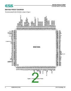
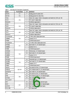
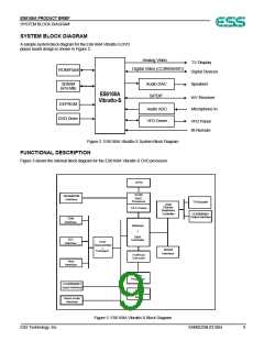
ES6168A PRODUCT BRIEF
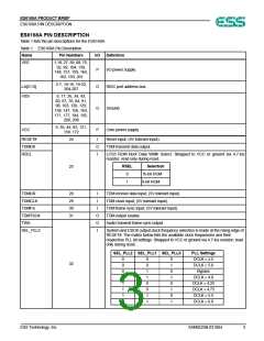
ES6168A PIN DESCRIPTION
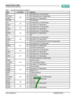
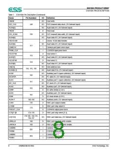
Table 1 ES6168A Pin Description (Continued)
Name
Pin Numbers
I/O
I/O
I/O
I/O
O
Definition
HWR#
Host write.
DCI_CLK
AUX4[5]
HRD#
149
DVD channel data clock; (5V tolerant input).
Aux4 data I/O; (5V tolerant input).
Host read.
DCI_ACK#
AUX4[6]
HIOCS16#
AUX3[4]
CAMCLK
PIXIN_CLK
HCS1FX#
AUX3[7]
HCS3FX#
AUX3[6]
HA[2:0]
150
151
I/O
I/O
I
DVD channel data valid; (5V tolerant input).
Aux4 data I/O; (5V tolerant input).
Device 16-bit data transfer.
Aux3 data I/O; (5V tolerant input).
Camera port pixel clock input.
CCIR656 input pixel clock.
Host select 1.
I/O
I
I
O
152
153
I/O
O
Aux3 data I/O; (5V tolerant input).
Host select 3.
I/O
I/O
I/O
I/O
I/O
I/O
I/O
I/O
O
Aux3 data I/O; (5V tolerant input).
Host address bus.
154, 155, 158
160
AUX4[4:2]
AUX0
Aux4 data I/Os; (5V tolerant input).
Auxiliary port 0 (open collector); (5V tolerant input).
I2C data I/O; (5V tolerant input).
Auxiliary port 1 (open collector); (5V tolerant input).
I2C clock I/O; (5V tolerant input).
Auxiliary port; (5V tolerant input).
I/O write strobe (LCS1).
I2CDATA
AUX1
161
I2C_CLK
AUX2
162
IOW#
AUX3
I/O
O
Auxiliary port; (5V tolerant input).
I/O read strobe (LCS1).
165
IOR#
AUX4-7
LOE#
166-169
170
I/O
O
Auxiliary ports; (5V tolerant input).
RISC port output enable.
LCS0#
O
RISC port chip select 0.
173
PIXOUT_CLK
LCS[3:1]#
O
CCIR656 output pixel clock.
RISC port chip select [3:1].
174-176
O
178-182, 185-191,
194-197
LD[15:0]
I/O
RISC port data bus; (5V tolerant input).
LWRLL#
LWRHL#
CAMIN0
PIXIN0
198
199
O
O
I
RISC port low-byte write enable.
RISC port high-byte write enable.
Camera YUV 0.
202
203
I
CCIR656 input pixel 0.
Camera YUV 1.
CAMIN1
PIXIN1
I
I
CCIR656 input pixel 1.
8
SAM0523B-031804
ESS Technology, Inc.

 ESS [ ESS Technology,Inc ]