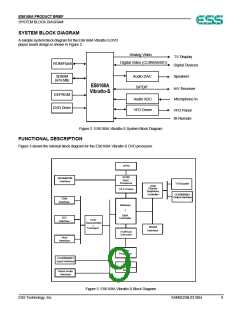
ES6168A PRODUCT BRIEF
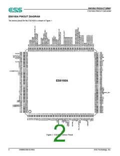
ES6168A PIN DESCRIPTION
ES6168A PIN DESCRIPTION
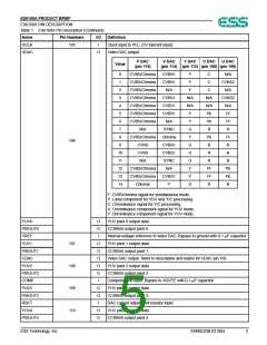
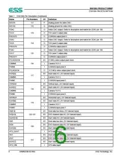
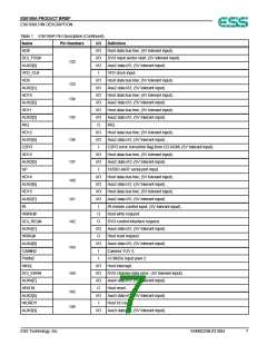
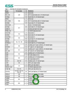
Table 1 lists the pin descriptions for the ES6168A.
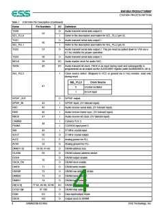
Table 1 ES6168A Pin Description
Name
Pin Numbers
I/O
Definition
VEE
1,18, 27, 59, 68, 75,
92, 99, 104, 130,
148, 157, 159, 164,
183, 193, 201
P
I/O power supply.
2-7, 10-16, 19-23,
204-207
LA[21:0]
VSS
O
G
P
RISC port address bus.
Ground.
8, 17, 26, 34, 43,
60, 67, 76, 84, 91,
98, 103, 120, 129,
138, 147, 156, 163,
171, 177, 184, 192,
200, 208
9, 35, 44, 83, 121,
139, 172
VCC
Core power supply.
RESET#
TDMDX
RSEL
24
I
O
I
Reset input; (5V tolerant input).
TDM transmit data output.
LCS3 ROM Boot Data Width Select. Strapped to VCC or ground via 4.7-kΩ
resistor; read only during reset.
RSEL
Selection
16-bit ROM
8-bit ROM
25
0
1
TDMDR
TDMCLK
TDMFS
28
29
30
31
I
I
TDM receive data input; (5V tolerant input).
TDM clock input; (5V tolerant input).
TDM frame sync input; (5V tolerant input).
TDM output enable.
I
TDMTSC#
TWS
O
O
I
Audio transmit frame sync output.
SEL_PLL2
System and DSCK output clock frequency selection is made at the rising edge of
RESET#. The matrix below lists the available clock frequencies and their
respective PLL bit settings. Strapped to VCC or ground via 4.7-kΩ resistor; read
only during reset.
SEL_PLL2 SEL_PLL1 SEL_PLL0
PLL Settings
DCLK × 4.5
DCLK × 5.0
Bypass
0
0
0
0
1
1
1
1
0
0
1
1
0
0
1
1
0
1
0
1
0
1
0
1
32
DCLK × 4.0
DCLK × 4.25
DCLK × 4.75
DCLK × 5.5
DCLK × 6.0
ESS Technology, Inc.
SAM0523B-031804
3

 ESS [ ESS Technology,Inc ]