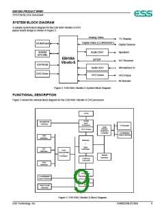
ES6168A PRODUCT BRIEF
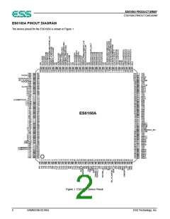
ES6168A PIN DESCRIPTION
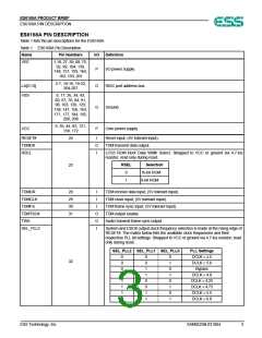
Table 1 ES6168A Pin Description (Continued)
Name
Pin Numbers
I/O
O
I
Definition
TSD0
Audio transmit serial data output 0.
33
SEL_PLL0
TSD1
Refer to the description and matrix for SEL_PLL2 pin 32.
Audio transmit serial data output 1.
O
I
36
37
SEL_PLL1
TSD2
Refer to the description and matrix for SEL_PLL2 pin 32.
O
Audio transmit serial data output 2. This pin must be pulled down to VSS via a
4.7-kΩ resistor for proper operation.
TSD3
MCLK
TBCK
38
39
40
O
Audio transmit serial data output 3.
Audio master clock for audio DAC.
I/O
I/O
Audio transmit bit clock. TBCK is an input during reset and subsequently is
programmed as an output via the AUDIOXMT register (addr 0x2000D00Ch, bit 4).
SEL_PLL3
I
Clock source select. Strapped to VCC or ground via 4.7-kΩ resistor; read only
during reset.
SEL_PLL3
Clock Source
Crystal oscillator
DCLK input
41
0
1
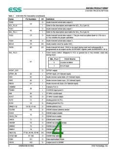
SPDIF_OUT
SPDIF_IN
RSD
O
I
S/PDIF output.
42
45
46
47
S/PDIF input; (5V tolerant input).
Audio receive serial data; (5V tolerant input).
Audio receive frame sync; (5V tolerant input).
Audio receive bit clock; (5V tolerant input).
Camera YUV 3.
I
RWS
I
RBCK
I
CAMIN3
PIXIN3
XIN
I
48
I
CCIR656 input pixel 3.
49
I
27-MHz crystal input.
XOUT
50
O
P
G
O
O
O
O
O
O
O
O
I/O
O
O
O
27-MHz crystal output.
AVEE
51
Analog power for PLL.
AVSS
52
53-58, 61-66
69
Analog ground for PLL.
DRAM address bus.
DMA[11:0]
DCAS#
DOE#
DRAM column address strobe.
DRAM output enable.
70
DSCK_EN
DWE#
DRAM clock enable.
71
DRAM write enable.
DRAS#
DMBS0
DMBS1
DB[15:0]
DCS[1:0]#
DQM
72
DRAM row address strobe.
DRAM bank select 0.
73
74
DRAM bank select 1.
77-82, 85-90, 93-96
DRAM data bus.
97,100
101
DRAM chip select.
Data input/output mask.
Output clock to DRAM.
DSCK
102
4
SAM0523B-031804
ESS Technology, Inc.

 ESS [ ESS Technology,Inc ]