ESMT
M14D5121632A (2H)
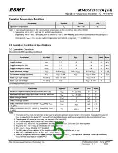
Operation Temperature Condition (TC) -40°C~95°C
DC Specifications
(IDD values are for the operation range of Voltage and Temperature)
Version
Unit
Parameter
Symbol
Test Condition
-1.8
-2.5
-3
One bank;
CK = tCK (IDD), tRC = tRC (IDD), tRAS = tRAS (IDD)min;
CKE is High, CS is HIGH between valid commands;
Address bus inputs are SWITCHING;
Data bus inputs are SWITCHING
One bank; IOUT = 0mA;
t
Operating Current
(Active - Precharge)
IDD0
100
90
80
mA
BL = 4, CL = CL(IDD), AL = 0;
t
t
CK = tCK (IDD), tRC = tRC (IDD),
RAS = tRAS (IDD)min, tRCD = tRCD (IDD);
Operating Current
(Active - Read -
Precharge)
IDD1
120
15
110
15
110
15
mA
mA
CKE is HIGH, CS is HIGH between valid commands;
Address bus inputs are SWITCHING;
Data pattern is same as IDD4W
All banks idle;
Precharge
Power-Down
Standby Current
tCK = tCK (IDD); CKE is LOW;
Other control and address bus inputs are STABLE;
Data bus inputs are FLOATING
IDD2P
IDD2Q
All banks idle;
t
Other control and address bus inputs are STABLE;
Data bus inputs are FLOATING
CK = tCK (IDD); CKE is HIGH, CS is HIGH;
Precharge Quiet
Standby Current
60
60
55
55
50
50
mA
mA
All banks idle;
tCK = tCK (IDD); CKE is HIGH, CS is HIGH;
Other control and address bus inputs are SWITCHING;
Idle Standby Current IDD2N
Data bus inputs are SWITCHING
All banks open;
CK = tCK (IDD); CKE is LOW;
Other control and address bus inputs
are STABLE;
Fast PDN Exit
MRS(12) = 0
75
25
65
25
60
25
t
Active Power-down
IDD3P
mA
mA
Standby Current
Slow PDN Exit
MRS(12) = 1
Data bus input are FLOATING
All banks open;
t
CK = tCK (IDD), tRAS = tRAS (IDD)max, tRP = tRP (IDD);
Active Standby
IDD3N
CKE is HIGH, CS is HIGH between valid commands;
Other control and address bus inputs are SWITCHING;
Data bus inputs are SWITCHING
95
80
75
Current
All banks open, continuous burst Reads, IOUT = 0mA;
BL = 4, CL = CL (IDD), AL = 0;
t
CK = tCK (IDD), tRAS = tRAS (IDD)max, tRP = tRP (IDD);
Operation Current
IDD4R
230
190
180
mA
mA
CKE is HIGH, CS is HIGH between valid commands;
Address bus inputs are SWITCHING;
(Read)
Data pattern is the same as IDD4W;
All banks open, continuous burst Writes;
BL = 4, CL = CL (IDD), AL = 0;
t
CKE is HIGH, CS is HIGH between valid commands;
Address bus inputs are SWITCHING;
CK = tCK (IDD), tRAS = tRAS (IDD)max, tRP = tRP (IDD);
Operation Current
IDD4W
240
200
190
(Write)
Data bus inputs are SWITCHING
Elite Semiconductor Memory Technology Inc.
Publication Date : Aug. 2011
Revision : 1.1 6/62

 ESMT [ ELITE SEMICONDUCTOR MEMORY TECHNOLOGY INC. ]