ESMT
M14D5121632A (2H)
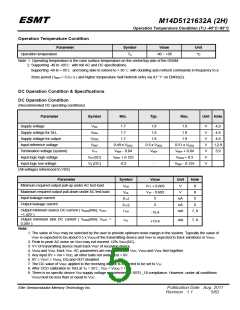
Operation Temperature Condition (TC) -40°C~95°C
AC Operation Conditions & Timing Specification
AC Operation Conditions
-1.8/ 2.5/ 3
Parameter
Symbol
Unit
Note
Min.
Max.
Input High (Logic 1) Voltage
Input Low (Logic 0) Voltage
Input Differential Voltage
VIH(AC)
VIL(AC)
VID(AC)
VIX(AC)
VREF + 0.2
V
V
V
V
V
VREF - 0.2
VDDQ+0.6
0.5
1
2
2
Input Crossing Point Voltage
0.5 x VDDQ - 0.175
0.5 x VDDQ - 0.125
0.5 x VDDQ + 0.175
0.5 x VDDQ + 0.125
Output Crossing Point Voltage VOX(AC)
Note:
1. VID(AC) specifies the input differential voltage |VTR – VCP| required for switching, where VTR is the true input signal (such
as CLK,DQS) and VCP is the complementary input signal (such as CLK , DQS ). The minimum value is equal to VIH(AC) –
VIL(AC).
2. The typical value of VIX / VOX(AC) is expected to be about 0.5 x VDDQ of the transmitting device and VIX / VOX(AC) is
expected to track variations in VDDQ. VIX / VOX(AC) indicates the voltage at which differential input / output signals must
cross.
Input / Output Capacitance
Parameter
Symbol
Min.
1.0
Max.
1.75
2.0
Unit Note
Input capacitance
-1.8/ 2.5
-3
CIN1
pF
pF
pF
1
1
2
(A0~A12, BA0~BA1, CKE, CS ,RAS , CAS , WE , ODT)
1.0
CIN2
1.0
2.5
2.0
3.5
Input capacitance (CLK, CLK )
-1.8/ 2.5/ 3
-1.8/ 2.5/ 3
CI / O
DQS, DQS & Data input/output capacitance
Input capacitance (DM)
CIN3
2.5
3.5
pF
2
Note: 1. Capacitance delta is 0.25 pF.
2. Capacitance delta is 0.5 pF.
Elite Semiconductor Memory Technology Inc.
Publication Date : Aug. 2011
Revision : 1.1 8/62

 ESMT [ ELITE SEMICONDUCTOR MEMORY TECHNOLOGY INC. ]