ESMT
M12L2561616A (2K)
AC OPERATING TEST CONDITIONS (VDD = 3.3V ± 0.3V ,TA = 0 to 70 °C )
Parameter
Input levels (Vih/Vil)
Value
2.4/0.4
1.4
Unit
V
Input timing measurement reference level
Input rise and fall-time
V
tr/tf = 1/1
1.4
ns
V
Output timing measurement reference level
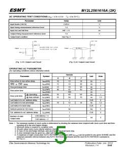
Output load condition
See Fig. 2
(Fig. 1) DC Output Load Circuit
(Fig. 2) AC Output Load Circuit
OPERATING AC PARAMETER
(AC operating conditions unless otherwise noted)
Version
Parameter
Symbol
Unit
Note
-5
10
15
-6
12
18
-7
14
20
Row active to row active delay
tRRD(min)
tRCD(min)
ns
ns
1
1
RAS to CAS delay
Row precharge time
tRP(min)
tRAS(min)
tRAS(max)
tRC(min)
15
40
18
42
20
45
ns
ns
us
ns
1
1
Row active time
100
60
@ Operating
Row cycle time
@ Auto refresh
55
55
63
70
1
tRFC(min)
60
ns
1,5
Last data in to col. address delay
Last data in to row precharge
tCDL(min)
tRDL(min)
1
CLK
ns
2
10
12
14
1,2
Last data in to burst stop
tBDL(min)
tREF(max)
tCCD(min)
1
64
1
CLK
ms
2
6
3
Refresh period (8,192 rows)
Col. address to col. address delay
CLK
CAS latency = 3
CAS latency = 2
2
Number of valid
Output data
ea
4
1
Note: 1. The minimum number of clock cycles is determined by dividing the minimum time required with clock cycle time and then
rounding off to the next higher integer.
2. Minimum delay is required to complete write.
3. All parts allow every cycle column address change.
4. In case of row precharge interrupt, auto precharge and read burst stop.
5. A new command may be given tRFC after self refresh exit.
6. A maximum of eight consecutive AUTO REFRESH commands (with tRFCmin) can be posted to any given SDRAM, and the
maximum absolute interval between any AUTO REFRESH command and the next AUTO REFRESH command is
8x7.8μ s.)
Elite Semiconductor Memory Technology Inc.
Publication Date: Jun. 2012
Revision: 1.4 5/45

 ESMT [ ELITE SEMICONDUCTOR MEMORY TECHNOLOGY INC. ]