Application Information: continued
Programmable Output
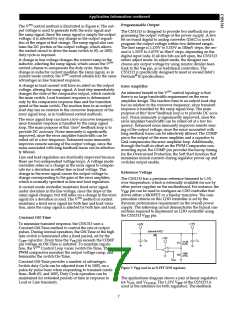
The V2TM control method is illustrated in Figure 6. The out-
put voltage is used to generate both the error signal and
the ramp signal. Since the ramp signal is simply the output
voltage, it is affected by any change in the output regard-
less of the origin of that change. The ramp signal also con-
tains the DC portion of the output voltage, which allows
the control circuit to drive the main switch to 0% or 100%
duty cycle as required.
The CS51313 is designed to provide two methods for pro-
gramming the output voltage of the power supply. A five
bit on board digital to analog converter (DAC) is used to
program the output voltage within two different ranges.
The first range is 2.125V to 3.525V in 100mV steps, the sec-
ond is 1.325V to 2.075V in 50mV steps, depending on the
digital input code. If all five bits are left open, the CS51313
enters adjust mode. In adjust mode, the designer can
choose any output voltage by using resistor divider feed-
back to the VFB pin, as in traditional controllers. The
CS51313 is specifically designed to meet or exceed Intel’s
Pentium® II specifications.
A change in line voltage changes the current ramp in the
TM
inductor, affecting the ramp signal, which causes the V2
control scheme to compensate the duty cycle. Since the
change in inductor current modifies the ramp signal, as in
current mode control, the V2TM control scheme has the same
advantages in line transient response.
A change in load current will have an affect on the output
voltage, altering the ramp signal. A load step immediately
changes the state of the comparator output, which controls
the main switch. Load transient response is determined
only by the comparator response time and the transition
speed of the main switch. The reaction time to an output
load step has no relation to the crossover frequency of the
error signal loop, as in traditional control methods.
The error signal loop can have a low crossover frequency,
since transient response is handled by the ramp signal
loop. The main purpose of this ‘slow’ feedback loop is to
provide DC accuracy. Noise immunity is significantly
improved, since the error amplifier bandwidth can be
rolled off at a low frequency. Enhanced noise immunity
improves remote sensing of the output voltage, since the
noise associated with long feedback traces can be effective-
ly filtered.
Line and load regulation are drastically improved because
there are two independent voltage loops. A voltage mode
controller relies on a change in the error signal to compen-
sate for a deviation in either line or load voltage. This
change in the error signal causes the output voltage to
change corresponding to the gain of the error amplifier,
which is normally specified as line and load regulation.
A current mode controller maintains fixed error signal
under deviation in the line voltage, since the slope of the
ramp signal changes, but still relies on a change in the error
signal for a deviation in load. The V2TM method of control
maintains a fixed error signal for both line and load varia-
tion, since the ramp signal is affected by both line and load.
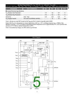
Error Amplifier
An inherent benefit of the V2TM control topology is that
there is no large bandwidth requirement on the error
amplifier design. The reaction time to an output load step
has no relation to the crossover frequency, since transient
response is handled by the ramp signal loop. The main
purpose of this”slow”feedback loop is to provide DC accu-
racy. Noise immunity is significantly improved, since the
error amplifier bandwidth can be rolled off at a low fre-
quency. Enhanced noise immunity improves remote sens-
ing of the output voltage, since the noise associated with
long feedback traces can be effectively filtered. The COMP
pin is the output of the error amplifier and a capacitor to
Gnd compensates the error amplifier loop. Additionally,
through the built-in offset on the PWM Comparator non-
inverting input, the COMP pin provides the hiccup timing
for the Overcurrent Protection, the Soft Start function that
minimizes inrush currents during regulator power-up and
switcher output enable.
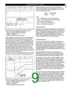
Reference Voltage
The CS51313 has a precision reference trimmed to 1.5%
over temperature, which is externally available for use by
other power supplies on the motherboard. For instance, the
VREF pin can be used to configure an LDO controller that
drives either a MOSFET or a bipolar transistor. The com-
pensation criteria on this LDO controller is set by the
dynamic performance requirement on the overall power
supply. The following circuit demonstrates the typical con-
nections required to implement an LDO controller using
the CS51313 VREF pin.
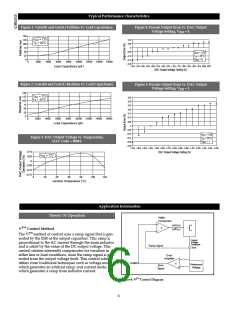
Constant Off-Time
+1.5V
To minimize transient response, the CS51313 uses a
Constant Off-Time method to control the rate of output
pulses. During normal operation, the Off-Time of the high
side switch is terminated after a fixed period, set by the
COFF capacitor. Every time the VFB pin exceeds the COMP
pin voltage an Off-Time is initiated. To maintain regula-
tion, the V2TM Control Loop varies switch On-Time. The
PWM comparator monitors the output voltage ramp, and
terminates the switch On-Time.
+3.3V
External N-FET
+12V
C
IN
C
O
21.9K
0.5%
R1
R2
-
+
100K
0.5%
V
REF
Constant Off-Time provides a number of advantages.
Switch duty Cycle can be adjusted from 0 to 100% on a
pulse-by pulse basis when responding to transient condi-
tions. Both 0% and 100% Duty Cycle operation can be
maintained for extended periods of time in response to
Load or Line transients.
Figure 7: VREF used in an N-FET LDO regulator.
The applications diagram shows a pair of linear regulators
for VGTL and VCLOCK. The 1.23V VREF of the CS51313 is
used as the reference for both regulators. The feedback
7

 CHERRY [ CHERRY SEMICONDUCTOR CORPORATION ]