Application Information: continued
resistors determine the output voltage for each regulator.
In this case, it will be 1.5V @ 3A for VGTL and 2.5V @ 1A for has achieved regulation and the initial pulse is then fol-
VCLOCK. In Figure 7 the ratio of resistor R1 to resistor R2 is lowed by a constant off time as programmed by the COFF
(VOUT/VREF) - 1, where VOUT = 1.5V and VREF = 1.23V. The capacitor. The COMP capacitor will continue to slowly
limit threshold voltage. In this case, the PWM control loop
same formula can be used to determine the ratio of the
feedback resistors needed to implement a 2.5V linear regu-
lator (VOUT = 2.5V).To negate the bias current of the opera-
charge and the regulator output voltage will follow it, less
the 1.1V PWM offset, until it achieves the voltage pro-
grammed by the DAC’s VID input. The Error Amp will
tional amplifier, a resistor with a value equal to the parallel then source or sink current to the COMP cap as required to
combination of the feedback resistors (R1//R2) is connect- maintain the correct regulator DC output voltage. Since the
ed in series with the non-inverting input of this operational rate of increase of the COMP pin voltage is typically set
amplifier. R2 sets the minimum output current, (IMIN
VREF/R2).
=
much slower than the regulator’s slew capability, inrush
current, output voltage, and duty cycle all gradually
increase from zero. (See Figures 8, 9, and 10).
The pass transistor must be able to dissipate the power
adequately while keeping the junction temperature below
the maximum specified by the manufacturer. For example,
with VGTL output of 1.5V, input voltage of 3.3V, and out-
put DC current of 3A, the pass transistor dissipates (3.3V -
1.5V) × 3A = 5.4W.
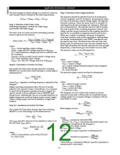
Start-up @
V
CC > 8.4V
Sufficient output capacitance must be added to ensure that
the output voltage remains within specification during
transient loading. For example, the GTL bus load can ramp
from 0 to 2.7A at a rate of 8A/µs. The designer needs to
verify that the circuit will meet these requirements using
the transistor and operational amplifier chosen.
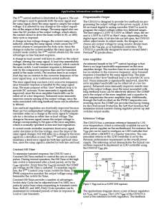
Startup
The CS51313 provides a controlled startup of regulator out-
put voltage and features Programmable Soft Start imple-
mented through the Error Amp and external Compensation
Capacitor. This feature, combined with overcurrent protec-
tion, prevents stress to the regulator power components
and overshoot of the output voltage during startup.
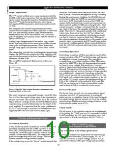
As Power is applied to the regulator, the CS51313
Figure 8: Normal Startup (2ms/div).
Channel 1 - Regulator Output Voltage (1V/div)
Channel 2 - COMP Pin (1V/div)
Channel 3 - VCC (10V/div)
Channel 4 - Regulator Input Voltage (5V/div)
Undervoltage Lockout circuit (UVL) monitors the IC’s sup-
ply voltage (VCC) which is typically connected to the +12V
output of the AC-DC power supply. The UVL circuit pre-
vents the NFET gates from being activated until VCC
exceeds the 8.4V (typ) threshold. Hysteresis of 300mV (typ)
is provided for noise immunity. The Error Amp Capacitor
connected to the COMP pin is charged by a 30µA current
source. This capacitor must be charged to 1.1V (typ) so that
TM
it exceeds the PWM comparator’s offset before the V2
PWM control loop permits switching to occur.
When VCC has exceeded 8.4V and COMP has charged to
1.1V, the upper Gate driver (GATE(H)) is activated, turn-
ing on the upper FET. This causes current to flow through
the output inductor and into the output capacitors and
load according to the following equation:
Start-up @
VCC > 8.4V
Initial Pulse until VOUT
> COMP + PWM Offset
T
I = (VIN – VOUT) ×
L
GATE(H) and the upper NFET remain on and inductor
current ramps up until the initial pulse is terminated by
either the PWM control loop or the overcurrent protection.
This initial surge of in-rush current minimizes startup time,
but avoids overstressing of the regulator’s power compo-
nents.
The PWM comparator will terminate the initial pulse if the
regulator output exceeds the voltage on the COMP pin
plus the 1.1V PWM comparator offset before the voltage
drop across the current sense resistor exceeds the current
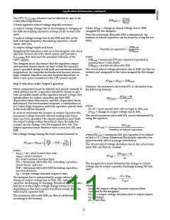
Figure 9: Normal Startup showing initial pulse followed by Soft Start
(20µs/div).
Channel 1 - Regulator Output Voltage (0.2V/div)
Channel 2 – Inductor Switching Node (5V/div)
Channel 3 - VCC (10V/div)
Channel 4 - Regulator Input Voltage (5V/div)
8

 CHERRY [ CHERRY SEMICONDUCTOR CORPORATION ]