TDA7851L
Electrical specifications
3
Electrical specifications
3.1
Absolute maximum ratings
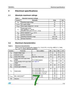
Table 3.
Symbol
Absolute maximum ratings
Parameter
Value
Unit
VS
Operating supply voltage
18
28
50
V
V
V
VS (DC) DC supply voltage
VS (pk) Peak supply voltage (for t = 50 ms)
Output peak current
IO
Non repetitive (t = 100 µs)
Repetitive (duty cycle 10 % at f = 10 Hz)
10
9
A
A
Ptot
Tj
Power dissipation Tcase = 70 °C
Junction temperature
85
W
°C
°C
°C
150
Tamb
Tstg
Operating temperature range
Storage temperature
-40 to 105
-55 to 150
3.2
Electrical characteristics
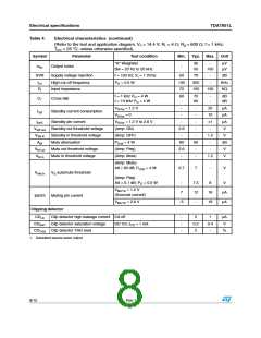
Table 4.
Electrical characteristics
(Refer to the test and application diagram, VS = 14.4 V; RL = 4 Ω; Rg = 600 Ω; f = 1 kHz;
amb = 25 °C; unless otherwise specified).
T
Symbol
Parameter
Test condition
Min.
Typ.
Max.
Unit
VS
Iq1
Supply voltage range
Quiescent current
-
8
-
150
-
18
V
RL = ∞
100
-60
300
+60
mA
mV
VOS
Output offset voltage
Play mode / Mute mode
During mute on/off output offset
voltage
-10
-
+10
+10
mV
mV
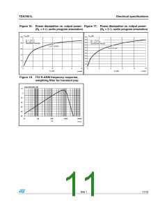
ITU R-ARM weighted
dVOS
see Figure 18
During standby on/off output offset
voltage
-10
25
-
Gv
Voltage gain
-
-
26
27
1
dB
dB
dGv
Channel gain unbalance
VS = 14.4 V; THD = 10 %
VS = 14.4 V; THD = 1 %
25
-
28
22
W
W
-
-
Po
Output power
VS = 14.4 V; THD = 10 %, 2 Ω
VS = 14.4 V; THD = 1 %, 2 Ω
48
38
W
W
-
VS = 14.4 V; RL = 4 Ω
VS = 14.4 V; RL = 2 Ω
45
75
W
W
Po max. Max. output power(1)
THD Distortion
-
-
-
Po = 4 W
0.01
0.05
%
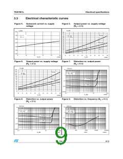
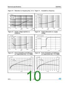
Rev 1
7/15

 ETC [ ETC ]