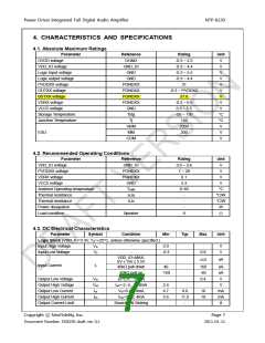
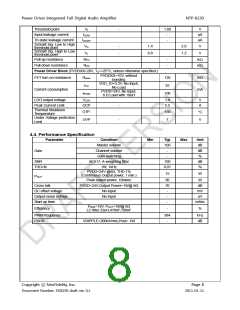
Power Driver Integrated Full Digital Audio Amplifier
NTP-8230
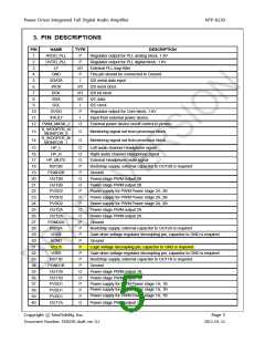
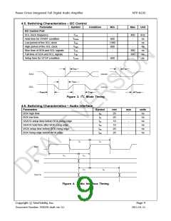
3. PIN DESCRIPTIONS
PIN
1
NAME
AVDD_PLL
DVDD_PLL
LF
TYPE
DESCRIPTION
Regulator output for PLL analog block, 1.8V
P
P
2
Regulator output for PLL digital block, 1.8V
External PLL loop filter
3
I/O
P
4
GND
This pin should be connected to Ground
I2S serial data input
5
SDATA
WCK
I
6
I/O
I/O
I/O
I
I2S word clock
7
BCK
I2S bit clock
8
SDA
I2C data
9
SCL
I2C clock
10
11
12
DVDD
P
Regulator output for Core block, 1.8V
Input from external power device
External power device on/off control to protect
/FAULT
PWM_MASK_2
I
O
S_WOOFER_A/
MONITOR_0
S_WOOFER_B/
MONITOR_1
13
14
O
O
Monitoring signal out from processor block
Monitoring signal out from processor block
15
16
17
18
19
20
21
22
23
24
25
26
27
28
29
30
31
32
33
34
35
36
37
38
39
40
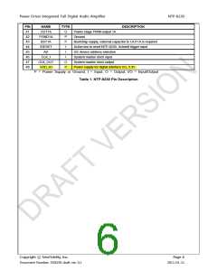
HP_L
HP_R
O
O
O
P
P
O
O
P
P
P
O
O
P
P
P
P
P
P
P
P
O
O
P
P
P
O
Left audio channel Headphone signal
Right audio channel Headphone signal
External Headphone mute signal
Bootstrap supply, external capacitor to OUT2B is required
Ground
HP_MUTE
BST2B
PGND2B
OUT2B
OUT2B
PVDD2
PVDD2
PVDD2
OUT2A
OUT2A
PGND2A
BST2A
VDR2
Power stage PWM output 2B
Power stage PWM output 2B
Power supply for PWM Power stage 2A, 2B
Power supply for PWM Power stage 2A, 2B
Power supply for PWM Power stage 2A, 2B
Power stage PWM output 2A
Power stage PWM output 2A
Ground
Bootstrap supply, external capacitor to OUT2A is required
Gate drive voltage regulator decoupling pin, capacitor to GND is required
Ground
AGND
VCC5
Logic voltage decoupling pin, capacitor to GND is required
Gate drive voltage regulator decoupling pin, capacitor to GND is required
Bootstrap supply, external capacitor to OUT1B is required
Ground
VDR1
BST1B
PGND1B
OUT1B
OUT1B
PVDD1
PVDD1
PVDD1
OUT1A
Power stage PWM output 1B
Power stage PWM output 1B
Power supply for PWM Power stage 1A, 1B
Power supply for PWM Power stage 1A, 1B
Power supply for PWM Power stage 1A, 1B
Power stage PWM output 1A
Copyright ⓒ NeoFidelity, Inc.
Document Number: DS8230 draft ver. 0.1
Page 5
2011-01-11

 ETC [ ETC ]