Power Driver Integrated Full Digital Audio Amplifier
NTP-8230
Table of Contents
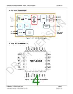
1. BLOCK DIAGRAM .......................................................................................................................................4
2. PIN ASSIGNMENTS.....................................................................................................................................4
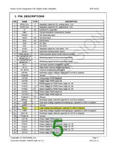
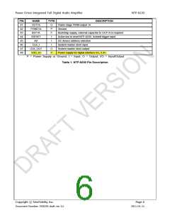
3. PIN DESCRIPTIONS....................................................................................................................................5
4. CHARACTERISTICS AND SPECIFICATIONS............................................................................................7
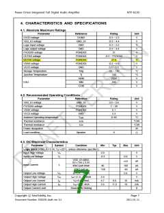
4.1. Absolute Maximum Ratings....................................................................................................................7
4.2. Recommended Operating Conditions ....................................................................................................7
4.3. DC Electrical Characteristics..................................................................................................................7
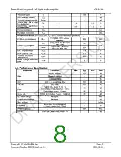
4.4. Performance Specification......................................................................................................................8
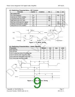
4.5. Switching Characteristics – I2C Control.................................................................................................9
4.6. Switching Characteristics – Audio Interface...........................................................................................9
5. I2C BUS OF NTP-8230 ............................................................................................................................. 10
5.1. General Description of I2C Bus........................................................................................................... 10
5.1.1. Writing Operation...............................................................................................................................11
5.1.2. Reading Operation ........................................................................................................................... 12
5.1.3. I2C Glitch Filter................................................................................................................................. 13
6. CLOCK, RESET & CONTROL.................................................................................................................. 14
6.1. System Clock....................................................................................................................................... 14
6.2. Reset Timing........................................................................................................................................ 14
7. AUDIO INPUT............................................................................................................................................ 15
7.1. I2S and Serial Audio Interface............................................................................................................. 15
8. MIXER........................................................................................................................................................ 17
9. PRE-PROCESSING .................................................................................................................................. 18
9.1. Pre Bi-Quad Filter Chain ..................................................................................................................... 18
9.2. 3D Surround ........................................................................................................................................ 18
9.3. Configurable Graphic Equalizer .......................................................................................................... 19
9.4. Post Bi-Quad Filter Chain.................................................................................................................... 19
9.5. Loudness Control ................................................................................................................................ 20
10. VOLUME & DYNAMIC RANGE CONTROL ............................................................................................. 21
10.1. Master Volume Control...................................................................................................................... 21
10.2. Channel Volume Control ................................................................................................................... 21
10.3. Master Volume Fine Control.............................................................................................................. 21
10.4. Mute and Soft Volume Change ......................................................................................................... 21
10.5. Auto Mute .......................................................................................................................................... 21
10.6. Dynamic Range Control .................................................................................................................... 22
11. OUTPUT INTERFACE............................................................................................................................... 23
11.1. Output Configuration.......................................................................................................................... 23
11.2. AM Interference Relief Mode............................................................................................................. 23
11.3. PWM Output Mapper......................................................................................................................... 23
11.4. Switching Output Mode ..................................................................................................................... 23
11.5. Soft start............................................................................................................................................. 24
12. TYPICAL APPLICATION SCHEMATICS (2CH Stereo) ........................................................................... 25
13. TYPICAL APPLICATION SCHEMATICS (2.1 Channel) .......................................................................... 26
14. APPENDIX................................................................................................................................................. 27
A. Configuration Register Summary....................................................................................................... 27
B. ROM address for BiQuads Coefficients and Parameters (Refer to Reg 0x7E) ................................. 43
C. Configuration Resister Value Reference ............................................................................................ 48
D. Outline and Mechanical Data ............................................................................................................. 54
Copyright ⓒ NeoFidelity, Inc.
Page 3
Document Number: DS8230 draft ver. 0.1
2011-01-11

 ETC [ ETC ]