Power Driver Integrated Full Digital Audio Amplifier
NTP-8230
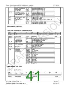
WTH
GFE
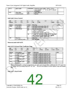
glitch width
b‟0000000 minimum pulse width = WTH + 20 ns
reset default = 1 * 10 ns (WTH default =
b‟1111111 b’0000001)
~
Glitch filter
enable/disable
b‟0
Glitch filter on
Bypass
b’1
Addr 0x62: Driver Control
Bit
7
6
5
4
3
2
1
0
Name
X
X
X
SB
PM
KMS
X
Name
KMS
Description
Fault glitch
elimination
Value Meaning
Ref.
b’0
b‟1
00
fault glitch elimination filter off
fault glitch elimination filter on
Normal Operation
PM
SB
PWM Mode
01
1 chip 2.1 channel mode
(Single Ended Mode)
cf) Should be disable 0x52 PSE
10
1 chip 2.0 channel mode or 2.1 channel
with external power stage (BTL Mode)
cf) Should be disable 0x4A SSE
Stand-by
Stand-by
0
in 2 channel mode
1
No stand-by
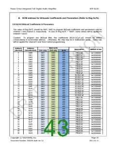
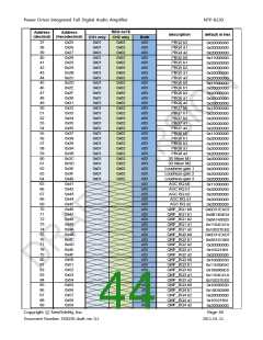
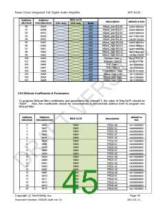
Reserved addr 0x63~0x7D
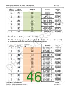
Addr 0x7E: Bi-Quad Filter Coefficient Page
Bit
7
6
5
4
3
2
1
0
Name
X
X
X
X
PEQ
CH3
CH2
CH1
Name
CH1
Description
Coefficient write
enable
Coefficient write
enable
Coefficient write
enable
Coefficient write
enable
Value
b’0
b‟1
b’0
b‟1
b’0
b‟1
b’0
b‟1
Meaning
Ref.
Disable coefficient write for ch1
Enable coefficient write for ch1
Disable coefficient write for ch2
Enable coefficient write for ch2
Disable coefficient write for ch3
Enable coefficient write for ch3
Disable coefficient write for PEQ
Enable coefficient write for PEQ
CH2
CH3
PEQ
Ref) In convenience, a device programmer can write same biquad filter coefficients for CH1 and CH2
at a single time by setting Reg 0x7E as “x03”. See the next pages to know register map and biquad
filter.
Addr 0x7F: Chip ID 0x99
Copyright ⓒ NeoFidelity, Inc.
Page 42
Document Number: DS8230 draft ver. 0.1
2011-01-11

 ETC [ ETC ]