SI-8000GL Series
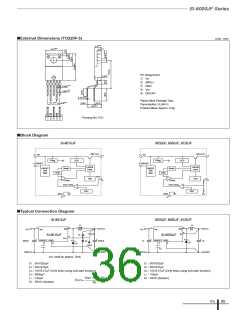
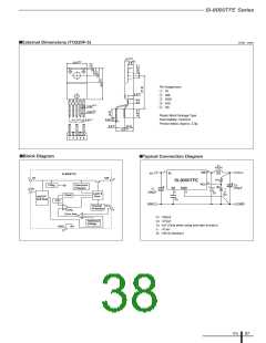
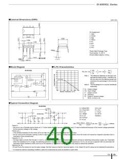
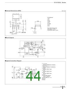
■External Dimensions (DIP8)
(Unit: mm)
8
7
6
5
Pin Assignment
1. GND
2. CE/SS
3. Reg
1
2
3
4
9.4±0.3
7.6
1.0+0.3
4. SWOUT
5. VIN
-
0.05
1.5+0.3
-
0.05
6. B.S
7. Comp
8. VREF
Plastic Mold Package Type
Flammability: UL 94V-0
Product Mass: Approx. 0.49 g
0.5±0.1
M
0.25
2.54
0° to 15°
0.89 TYP
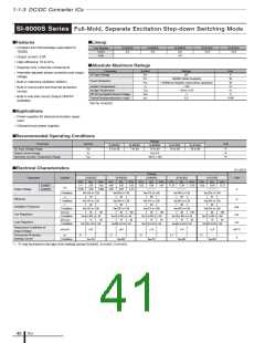
■Block Diagram
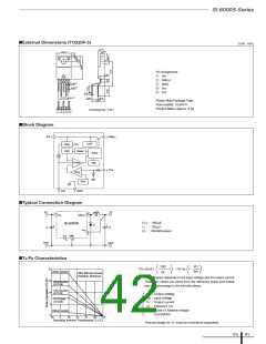
■Ta-PD Characteristics
2
1.8
1.6
1.4
1.2
SI-8010GL
100
VO
PD=VO • IO
–1 –VF • IO 1–
ηχ
VIN
V
IN
Note 1: The efficiency depends on the input volt-
age and the output current. Therefore, ob-
tain the value from the efficiency graph and
substitute the percentage in the formula
above.
UVLO
CE/SS
TSD
P.REG
OCP
CE/SS
θj-a:100°C/W
BS
Boot REG
1
0.8
0.6
0.4
0.2
0
DRIVE
Note 2: Thermal design for D1 must be considered
separately.
Reg
+
OSC
PWM
LOGIC
SWOUT
-
VO : Output voltage
VIN : Input voltage
IO : Output current
ηχ : Efficiency
V
REF
–25
0
25
50
75
100
(°C)
125
Comp
-
Amp
+
Ambient Temperature T
a
1V
GND
VF : Diode D1 forward voltage
RK16···0.4V(IO=1A)
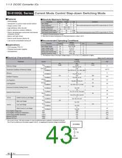
■Typical Connection Diagram
SI-8010GL
C1: 220µF/63V
C8: 0.1µF
R1: 47Ω
6
R1
4
C2: 470µF/25V
C3: 0.1µF
B.S
L1
L1: 47µH
D1: RK16
(Sanken)
C3
D1
5
V
IN
VIN
SWOUT
V0
C4: 1000pF
C5: 0.1µF
SI-8010GL
2
CE/SS
Reg
R2
+
+
C1
C7
VREF
C6: 0.047µF
C7: 0.1µF
Comp
7
GND
1
C2
C8
8
I
REF
R3
3
C4
C5
C6
(VOUT–VREF) (VOUT–1)
VREF
1
.
GND
GND
=
500(Ω)
.
R2=
=
(Ω), R3 =
=
IREF
2×10⁻³
IREF
2×10⁻³
Diode D1
• Be sure to use a Schottky-barrier diode as D1. If other diodes like fast recovery diodes are used, IC may be destroyed because of the reverse voltage generated
by the recovery voltage or ON voltage.
Choke coil L1
• If the winding resistance of the choke coil is too high, the efficiency may drop below the rated value.
• As the overcurrent protection starting current is approx. 2.5 A, take care concerning heat radiation from the choke coil caused by magnetic saturation due to
overload or short-circuited load.
Capacitor C1, C2
• As large ripple currents flow through C1 and C2, use high-frequency and low-impedance capacitors aiming for switching-mode-power-supply use. Especially
when the impedance of C2 is high, the switching waveform may become abnormal at low temperatures. For C2, do not use a capacitor with an extremely low
equivalent series resistance (ESR) such as an OS capacitor or a tantalum capacitor, which may cause an abnormal oscillation.
Resistors R2, R3
• R2 and R3 are the resistors to set the output voltage. Set their values so that IREF becomes approx. 2 mA. Obtain R2 and R3 values by the following formula above.
* To create the optimum operating conditions, place the components as close as possible to each other.
ICs
39

 ETC [ ETC ]