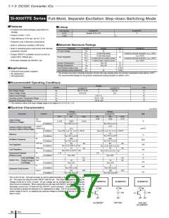
1-1-3 DC/DC Converter ICs
SI-8000GL Series Compact, Separate Excitation Step-down Switching Mode
■Features
• DIP 8 pin package
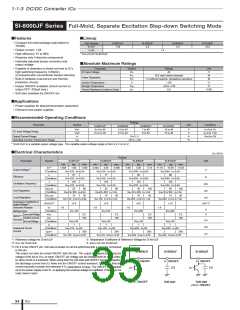
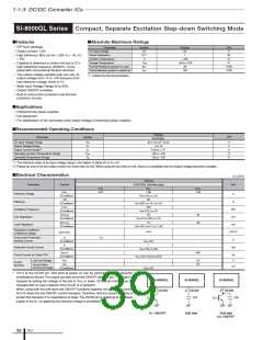
■Absolute Maximum Ratings
Parameter
Symbol
Ratings
Unit
V
• Output current: 1.5A
DC Input Voltage
VIN
53
*1
Power Dissipation
PD
1
+125
W
• High efficiency: 86% (at VIN = 20V, lO = 1A, VO
= 5V)
Junction Temperature
Tj
°C
Storage Temperature
Tstg
θj-c
θj-a
–40 to +125
28
°C
• Capable of downsize a choke-coil due to IC's
high switching frequency (250kHz). (Com-
pared with conventional Sanken devices)
Thermal Resistance (junction to case)
Thermal Resistance (junction to ambient air)
°C/W
°C/W
100
• The output-voltage-variable type can vary its
output voltage from 1V to 14V because of its
low reference voltage (Vref) of 1V.
*1: Limited by thermal protection.
• Wide Input Voltage Range (8 to 50V)
• Output ON/OFF available
• Built-in overcurrent protection and thermal
protection circuits
■Applications
• Onboard local power supplies
• OA equipment
• For stabilization of the secondary-side output voltage of switching power supplies
■Recommended Operating Conditions
Ratings
Unit
Parameter
Symbol
SI-8010GL
DC Input Voltage Range
VIN
VO
IO
(8 or VO+3)*1 to 50
V
V
Output Voltage Range
Output Current Range*2
1 to 14
0.02 to 1.5*2
–30 to +125
–30 to +125
A
Operating Junction Temperature Range
Operating Temperature Range
Tjop
Top
°C
°C
*1: The minimum value of an input voltage range is the higher of either 8V or VO+3V.
*2: Please be sure to let the output current run more than 20 mA. When using by less than 20 mA, there is a possibility that the output voltage becomes unstable.
■Electrical Characteristics
(Ta=25°C)
Ratings
Parameter
Symbol
SI-8010GL (Variable type)
Unit
min.
0.97
typ.
max.
1.03
VREF
1.00
Reference Voltage
V
Conditions
Eff
VIN=12V, IO=1A
86
Efficiency
%
Conditions
FOSC
VIN=20V, IO=1A, VO=5V
250
VIN=12V, IO=1A
20
Oscillation Frequency
Line Regulation
Load Regulation
kHZ
mV
Conditions
∆VOLINE
40
30
Conditions
∆VOLOAD
Conditions
VIN=10 to 30V, IO=1A
10
mV
VIN=12V, IO=0.1 to 1.5A
Temperature Coefficient
of Reference Voltage
±0.5
mV/°C
∆VREF/∆Ta
Overcurrent Protection
Starting Current
IS
1.6
A
Conditions
Iq
VIN=12V
7
Quiescent Circuit Current
mA
Conditions
Iq(OFF)
VIN=12V, IO=0A
400
Circuit Current at Output OFF
µA
V
Conditions
VSSL
VIN=12V, VON/OFF=0.3V
VSSL=0V
Low Level Voltage
CE/SS*
0.5
50
ISSL
Terminal Outflow
Current at Low Voltage
Terminal
µA
Conditions
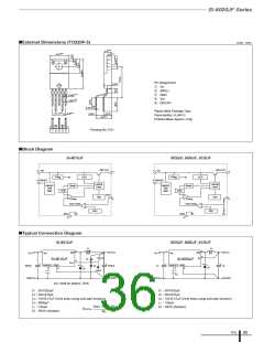
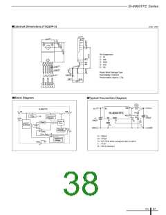
*: Pin 2 is the CE/SS pin. Soft start at power on can be performed with a capacitor
connected to this pin.The output can also be turned ON/OFF with this pin. The output is
stopped by setting the voltage of this pin to VSSL or lower. CE/SS-pin voltage can be
changed with an open-collector drive circuit of a transistor.
SI-8000GL
SI-8000GL
SI-8000GL
When using both the soft-start and ON/OFF functions together, the discharge current
from C4 flows into the ON/OFF control transistor. Therefore, limit the current securely to
protect the transistor if C3 capacitance is large. The CE/SS pin is pulled up to the power
supply in the IC, so applying the external voltage is prohibited.
2
CE/SS
2
CE/SS
C4
2 CE/SS
C4
VO. ON/OFF
Soft start
Soft start
+VO. ON/OFF
ICs
38

 ETC [ ETC ]